Multi-layer floating gate nonvolatile memory structure and production method thereof

A non-volatile, manufacturing method technology, applied in semiconductor/solid-state device manufacturing, coating, electric solid-state devices, etc., can solve problems such as insufficient charge storage capacity, improve yield, improve retention characteristics, and increase storage window effect

Inactive Publication Date: 2010-08-25
INST OF MICROELECTRONICS CHINESE ACAD OF SCI
View PDF0 Cites 7 Cited by
  • Summary
  • Abstract
  • Description
  • Claims
  • Application Information

AI Technical Summary

Problems solved by technology

[0005] However, in the second scheme, there is also the problem of insufficient charge storage capacity for silicon nanocrystal floating gate memory, and the use of multi-layer structure can improve the charge storage capacity of nanocrystals, and can also be used for multi-bit storage

Method used


Image

  • Multi-layer floating gate nonvolatile memory structure and production method thereof
  • Multi-layer floating gate nonvolatile memory structure and production method thereof
  • Multi-layer floating gate nonvolatile memory structure and production method thereof

Examples


Embodiment Construction

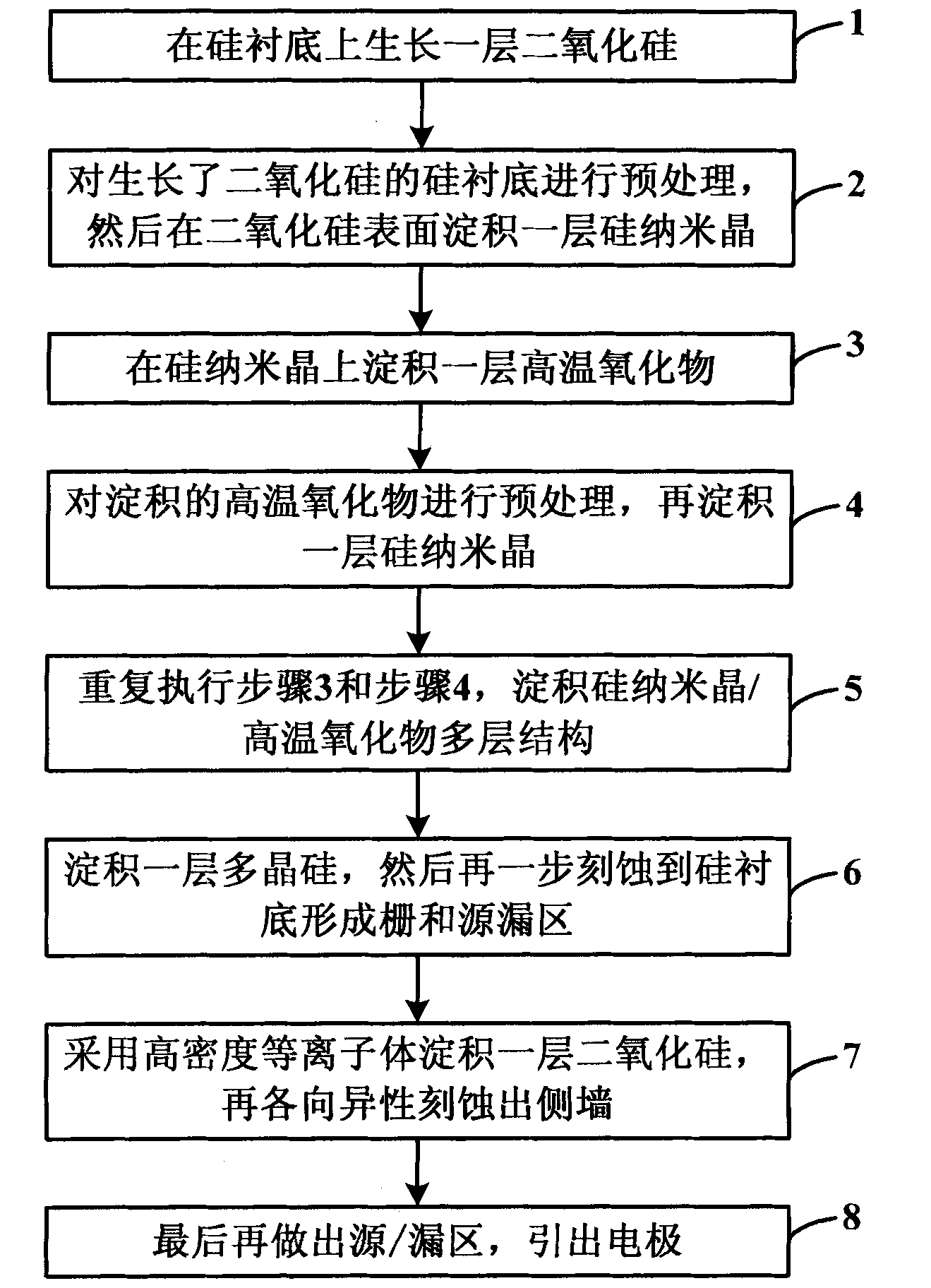
[0036] In order to make the object, technical solution and advantages of the present invention clearer, the present invention will be described in further detail below in conjunction with specific embodiments and with reference to the accompanying drawings.

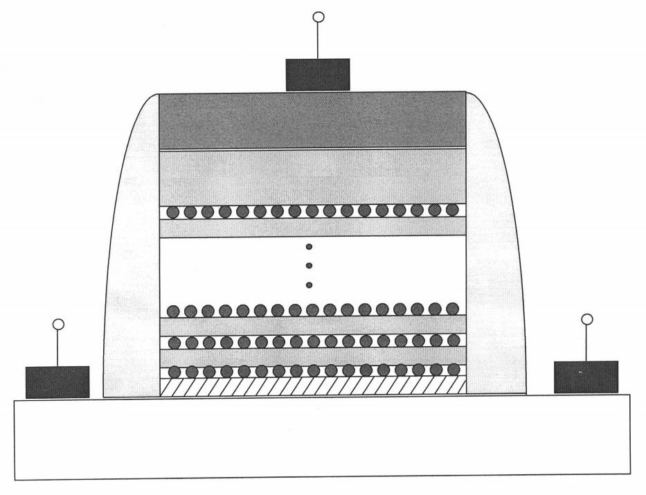
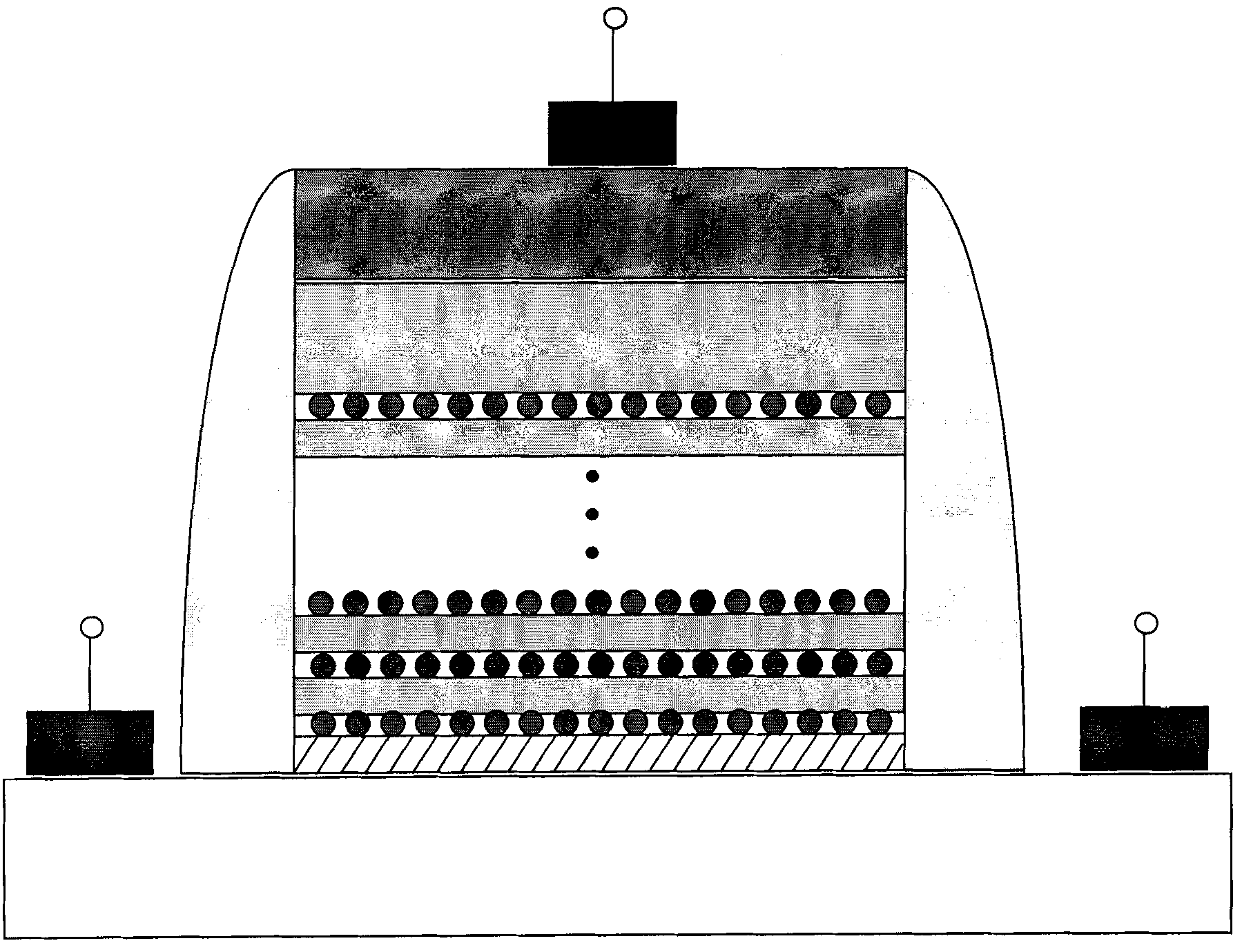
[0037] The invention is a multi-layer floating gate structure in a non-volatile memory using silicon nanocrystals as a storage medium, which can improve the ability of the floating gate layer to store charges, thereby increasing the storage window.

[0038] As shown in Figure 1, Figure 1 is a structural schematic diagram of a multilayer floating gate nonvolatile memory structure provided by the present invention, which comprises a silicon substrate, a silicon dioxide layer, silicon nanocrystals / high temperature oxide from bottom to top in sequence A multi-layer structure, a polysilicon layer, a silicon dioxide layer, a gate and a source / drain region formed by etching on a silicon substrate, and a side wall formed by etchin...


PUM

PropertyMeasurementUnit
thicknessaaaaaaaaaa
thicknessaaaaaaaaaa
thicknessaaaaaaaaaa

Abstract

The invention discloses a multi-layer floating gate nonvolatile memory structure and a production method thereof, wherein the multi-layer floating gate nonvolatile memory structure comprises a silicon substrate, a silicon dioxide layer, a silicon nanocrystals / high temperature oxide multilayer structure, a polysilicon layer, a silicon dioxide layer, grid and source / drain region formed by sculpturing on the silicon substrate, and a side wall formed by sculpturing on the silicon dioxide layer. The invention solves the defects because the traditional Flash technology node can downsized, utilizes the multi-layer floating gate to storage charge to enhance a storage window, so that the reliability of the floating grid for storing charge can be increased and the retention performance of a floating device can be improved.

Description

technical field [0001] The invention relates to the technical field of semiconductor devices, in particular to a multi-layer floating gate nonvolatile memory structure using silicon nanocrystals as a storage medium and a manufacturing method thereof. Background technique [0002] Since D.Kahng and S.M.Sze of Bell Laboratories proposed the nonvolatile semiconductor memory with floating gate structure in 1967, the floating gate semiconductor memory based on the gate stacked MOSFET structure occupies an extremely high capacity, cost and power consumption. The big advantage replaced the magnetic memory that had been used for a long time before. [0003] On this basis, Japan's Toshiba Corporation successfully proposed the concept of Flash memory in 1984. At present, Flash memory is the mainstream device in the non-volatile semiconductor memory market. However, with the continuous advancement of microelectronic technology nodes, the process line width will Further reduction, the ...

Claims


Application Information

Patent Timeline
Patent Type & Authority Applications(China)
IPC IPC(8): H01L27/115H01L21/8247H01L21/283H01L21/205C23C16/24
Inventor 刘明王永王琴杨潇楠
Owner INST OF MICROELECTRONICS CHINESE ACAD OF SCI
Why Eureka
Try Eureka