ABO3/TiO2/MgO/III-V group nitride semiconductor heterostructure and preparation method
What is AI technical title?
AI technical title is built by Patsnap AI team. It summarizes the technical point description of the patent document.
A nitride semiconductor, heterostructure technology, applied in the field of microelectronic materials, to achieve the effect of reducing leakage current
Inactive Publication Date: 2011-12-28
UNIV OF ELECTRONICS SCI & TECH OF CHINA
View PDF0 Cites 0 Cited by
Summary
Abstract
Description
Claims
Application Information
AI Technical Summary
This helps you quickly interpret patents by identifying the three key elements:
Problems solved by technology
Method used
Benefits of technology
Problems solved by technology
Therefore, it is proposed to use TiO 2 / MgO composite buffer layer to prepare ABO 3 / TiO 2 / MgO / hexagonal III-V nitride semiconductor heterojunction method, there is no similar report at home and abroad
Method used
Image
Click on the blue label to locate the original text in one second.
Reading with bidirectional positioning of images and text.
Examples
Embodiment 1
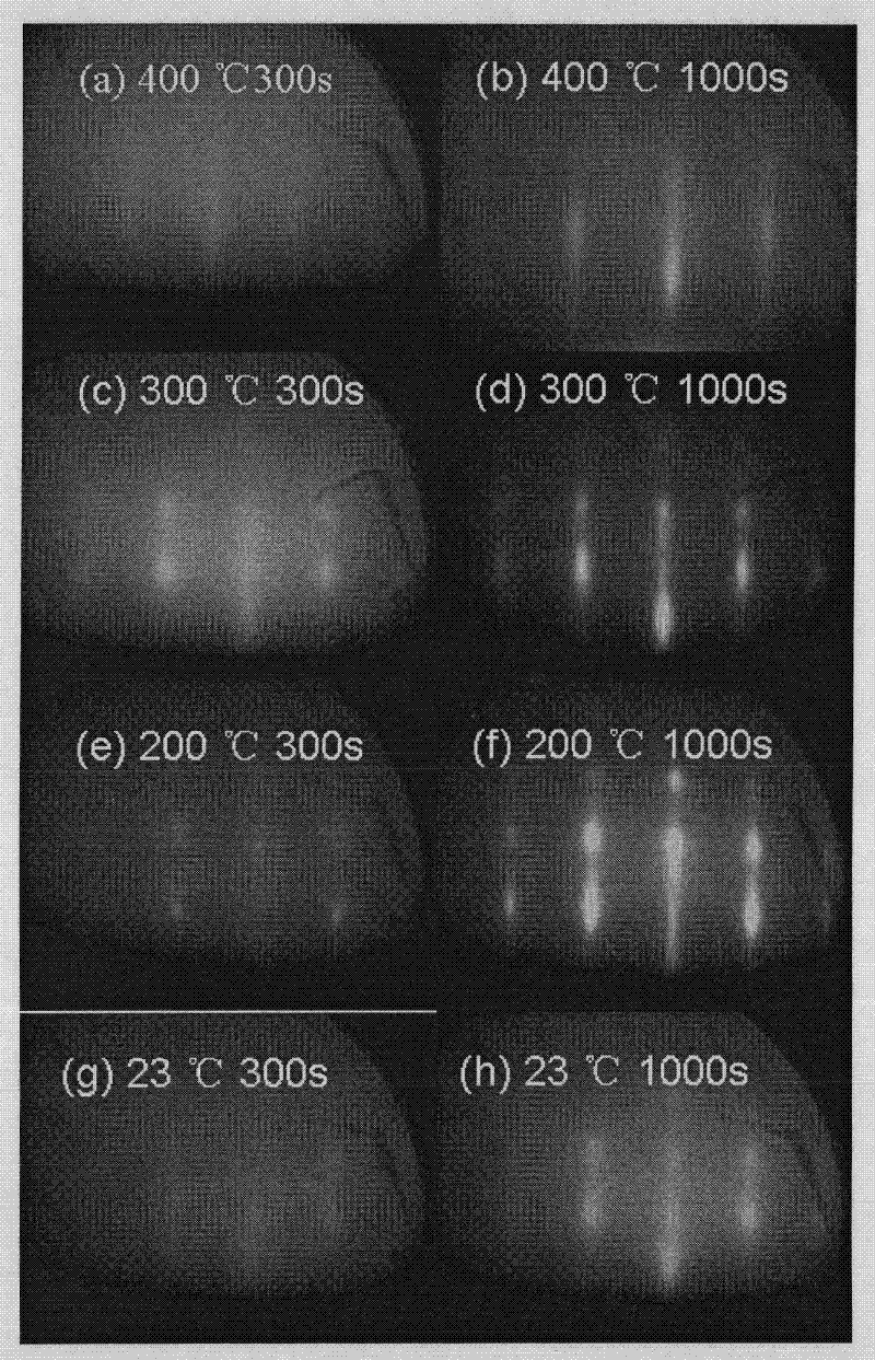
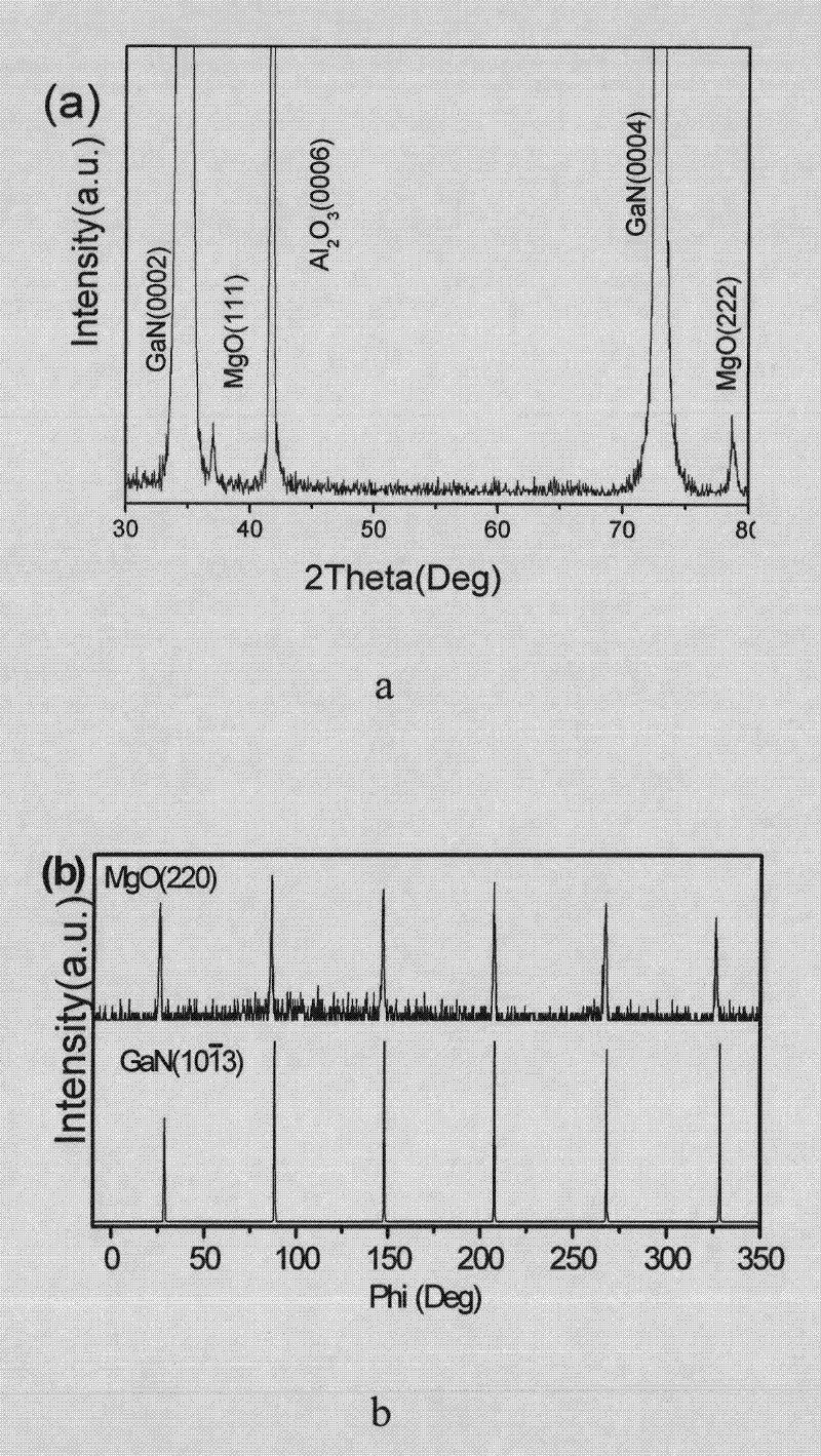
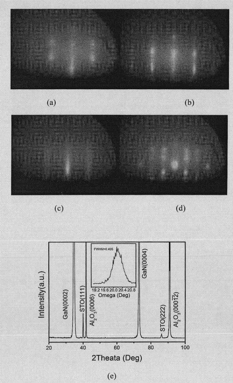
[0040] Such as Figure 8 , the ABO of this example 3 / TiO 2 / MgO / hexagonal III-nitride semiconductor heterostructure has three layers, on the semiconductor substrate and ABO 3 Between the oxide film functional layers, there is a MgO barrier layer and TiO 2 Composite buffer layer composed of template layer.
[0041] The hexagonal III-V nitride semiconductor is oriented in the (0001) direction. The MgO barrier layer is oriented along the (111) direction, and the TiO 2 The template layer is oriented along the (200) direction, while the ABO 3 The functional oxide film is oriented along the (111) direction. ABOs 3 In the metal oxide, A is an element among Mg, Ca, Sr, Ba, Pb, Bi, and La, and B is an element among Ti, Zr, Fe, Ru, and Ni.
Embodiment 2
[0043] The difference between this example and Example 1 is that A is a solid solution composed of two or more elements in Mg, Ca, Sr, Ba, Pb, Bi, La, and B is Ti, Zr, Fe, Ru, Ni A solid solution composed of two or more elements in , and, based on the molar ratio of A element, B element and oxygen element, the stoichiometric ratio satisfies (A 1 +A 2 +......+An): (B 1 +B 2 +...+Bn):O=1:1:3.
[0044] ABOs 3 Metal oxides can be doped with a certain proportion of modified oxides, namely RE A oxide or RE B oxides, the stoichiometric ratio satisfies (A 1 +A 2 +......+An+RE A ): (B 1 +B 2 +......+Bn+RE B ):O=1:1:3, where RE A and RE B Each represents an element in La, Ce, Pr, Nd, Pm, Sm, Eu, Gd, Tb, Dy, Ho, Er, Tm, Yb, Lu, Y, Mn.
[0045] As an embodiment of the preparation method, using lasermolecular beamepitaxy (L-MBE), using GaN / Al 2 o 3 and AlGaN / GaN / Al 2 o 3 Epitaxial wafer and MgO, TiO 2 and STO ceramic target, MgO barrier layer, TiO 2 Template layers an...
PUM
Property
Measurement
Unit
thickness
aaaaa
aaaaa
thickness
aaaaa
aaaaa
Abstract
The invention discloses an ABO3 / TiO2 / MgO / III-V group nitridesemiconductor heterostructure and a preparation method, relating to the field of microelectronic materials. The semiconductor heterostructure comprises a semiconductor substrate and an ABO3 perovskite structure functional oxide film. The semiconductor heterostructure is characterized in that a compound buffer layer formed by a TiO2 template layer of a nano thickness and an MgO barrier layer is arranged between the substrate and the functional oxide film. The TiO2 / MgO compound buffer layer with good epitaxial quality is prepared on aGaN epitaxial wafer through a mode of lasermolecular beamepitaxy at low temperature for the first time by the invention, wherein the MgO layer has the effect of the barrier layer, and the TiO2 is used as the template layer and can effectively induce the epitaxial growth of the ABO3 film.
Description
technical field [0001] The invention relates to the field of microelectronic materials, in particular to the band matching between oxides and wide bandgap semiconductors and the growth orientation of oxide films used in the integration of perovskite oxide functional materials and hexagonal III-V nitride semiconductor wide bandgap semiconductors Heterojunction structure design and preparation technology. Background technique [0002] Hexagonal III-V nitride semiconductors such as GaN, AlN, and InN are typical third-generation wide bandgap semiconductors, which have wide bandgap width, high breakdown electric field, large thermal conductivity, high carrier mobility, and radiation resistance. Strong ability and other characteristics, it has a wide range of applications in microelectronics and optoelectronic devices. Since GaN, AlN, etc. have certain piezoelectric polarization and spontaneous polarization, the AlGaN / GaN structure can form a concentration as high as 10 13 cm -...
Claims
Application Information
Patent Timeline
Application Date:The date an application was filed.
Publication Date:The date a patent or application was officially published.
First Publication Date:The earliest publication date of a patent with the same application number.
Issue Date:Publication date of the patent grant document.
PCT Entry Date:The Entry date of PCT National Phase.
Estimated Expiry Date:The statutory expiry date of a patent right according to the Patent Law, and it is the longest term of protection that the patent right can achieve without the termination of the patent right due to other reasons(Term extension factor has been taken into account ).
Invalid Date:Actual expiry date is based on effective date or publication date of legal transaction data of invalid patent.

