Method for preparing transistor device of crystallized thin film

A transistor and amorphous silicon thin film technology, applied in the field of polysilicon thin film preparation, can solve the problems of polysilicon thin film preparation process complexity, poor performance, and many residues, and achieve the effect of eliminating the misalignment of the alignment plate and shortening the process time

Inactive Publication Date: 2010-09-15
GUANGDONG SINODISPLAY TECH
View PDF1 Cites 16 Cited by
  • Summary
  • Abstract
  • Description
  • Claims
  • Application Information

AI Technical Summary

Problems solved by technology

[0007] In order to overcome the defects of complex preparation process, many residues and poor performance of the polysilicon thin...

Method used


Image

  • Method for preparing transistor device of crystallized thin film
  • Method for preparing transistor device of crystallized thin film
  • Method for preparing transistor device of crystallized thin film

Examples


preparation example Construction

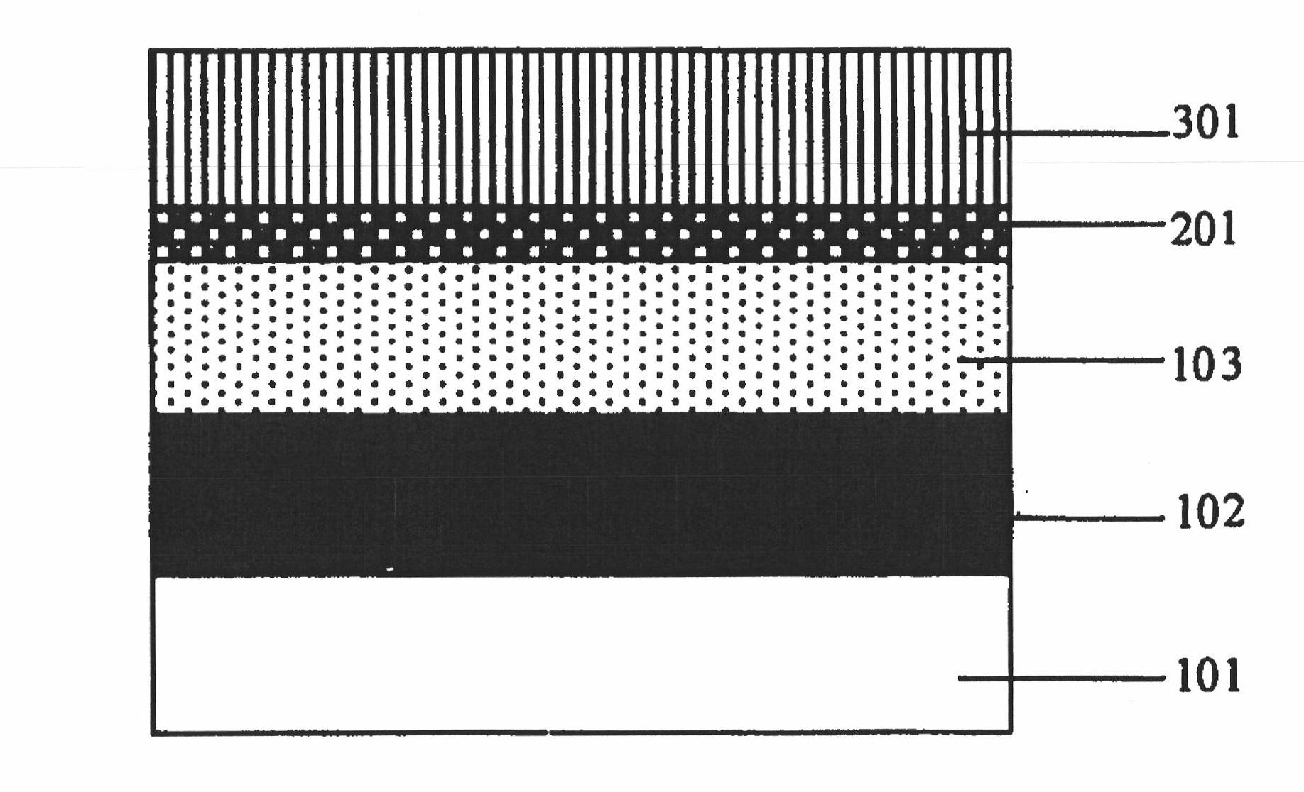
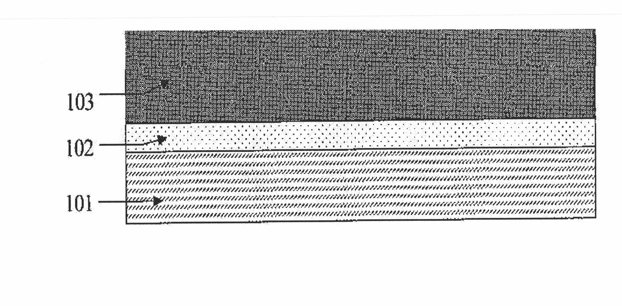
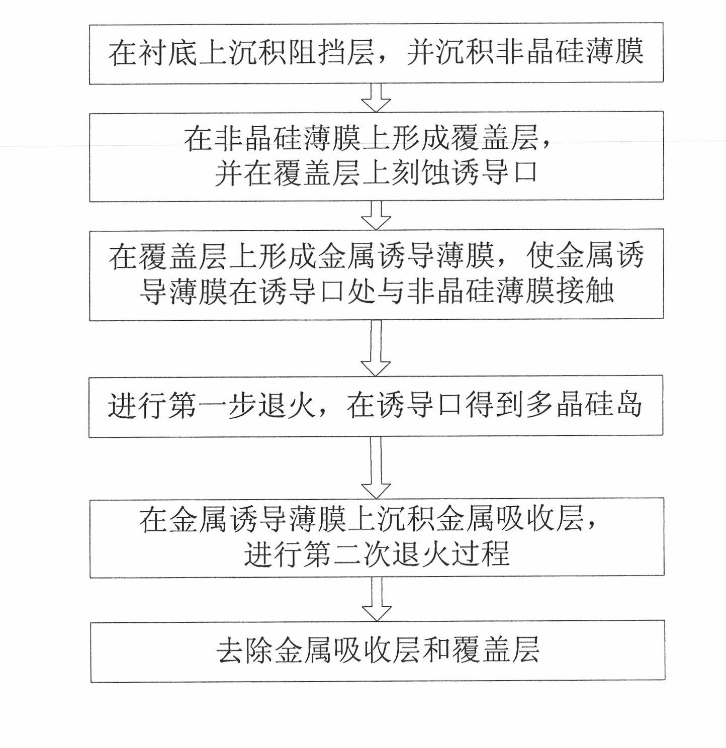
[0020] image 3 A flowchart showing a method for preparing a polysilicon thin film according to an embodiment of the present invention. In general, if image 3 As shown, the method includes: depositing a silicon oxide or silicon nitride barrier layer on a glass substrate, and depositing an amorphous silicon film (step 301); forming a layer of silicon oxide or silicon nitride capping layer on the amorphous silicon film , and etch the induction port (step 302) on the cover layer; form a layer of metal induction film on the cover layer, make the metal induction film contact with the amorphous silicon film at the induction port (step 303); carry out the first step Annealing process, polysilicon islands are obtained in the amorphous silicon film below the induction port (step 304); a metal absorption layer is deposited on the metal induction film, and then the second annealing process is performed to form crystallized amorphous with uniform distribution of crystal grains Silicon ...


PUM

PropertyMeasurementUnit
Thicknessaaaaaaaaaa
Thicknessaaaaaaaaaa

Abstract

The invention provides a method for preparing a transistor device. The preparation method comprises the following steps of: settling a blocking layer on a glass substrate and settling a non-crystalline silicon thin film; forming a covering layer on the non-crystalline silicon thin film and etching an induction port on the covering layer; forming a metal induction thin film on the covering layer, so that the metal induction thin film is contacted with the non-crystalline silicon thin film at the induction port; annealing for the first time to obtain a polysilicon island from the non-crystalline silicon thin film under the induction port; settling a metal absorbing layer on the metal induction thin film and annealing for the second time to form a crystallized thin film with crystalline grains distributed uniformly; removing the metal absorbing layer and the covering layer to obtain a polysilicon thin film; processing an active island pattern of a non-crystalline silicon thin film transistor (TFT) by using the polysilicon thin film; and forming a gate electrode, settling an insulating layer, opening contact holes of the grate electrode, the source electrode and the drain electrode, sputtering the metal electrodes, and settling metal interconnecting layer.

Description

technical field [0001] The invention relates to the technical field of polysilicon thin film preparation, and more specifically, the invention relates to a method for preparing a crystallized thin film transistor device. Background technique [0002] The preparation process of amorphous silicon thin film transistor (TFT) is mature and relatively simple, with high yield and low cost. Most of the existing active matrix displays use amorphous silicon thin film transistors. However, amorphous silicon thin film transistors have low field-effect mobility and poor device stability, making it difficult to meet the requirements of fast-switching color sequential liquid crystal displays, current-driven organic light-emitting diode displays, and integrated displays. The low-temperature polysilicon thin film transistor prepared on the glass substrate and obtained by annealing furnace or laser heating has high mobility and good device stability, and is suitable for the preparation of fas...

Claims


Application Information

Patent Timeline
IPC IPC(8): H01L21/336H01L21/20
Inventor 黄宇华黄飚彭俊华
Owner GUANGDONG SINODISPLAY TECH
Why Eureka
Try Eureka