Method for manufacturing three-dimensionally stacked resistance conversion memory

A resistance conversion, three-dimensional technology, applied in semiconductor/solid-state device manufacturing, electric solid-state devices, semiconductor devices, etc., can solve the problem of resistance conversion memory without a good technical route, and achieve the effect of less defects and good reliability

Active Publication Date: 2010-09-15
SHANGHAI INST OF MICROSYSTEM & INFORMATION TECH CHINESE ACAD OF SCI
View PDF6 Cites 10 Cited by
  • Summary
  • Abstract
  • Description
  • Claims
  • Application Information

AI Technical Summary

Problems solved by technology

At present, there is no good technical route for th

Method used


Image

  • Method for manufacturing three-dimensionally stacked resistance conversion memory
  • Method for manufacturing three-dimensionally stacked resistance conversion memory
  • Method for manufacturing three-dimensionally stacked resistance conversion memory

Examples


Embodiment 1

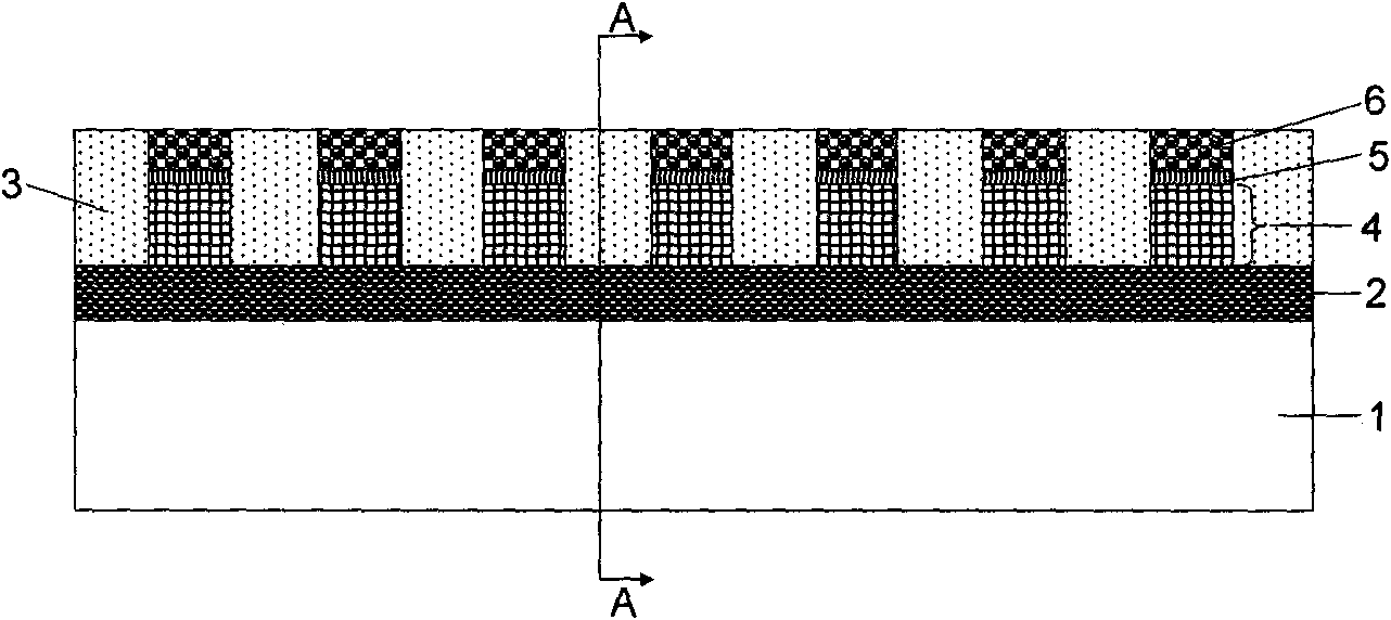
[0052] Please refer to FIG. 1, the present invention discloses a method for manufacturing a three-dimensional stacked resistance switching memory, including the following steps:

[0053] (1) Figure 1A Shown is the substrate manufactured with peripheral circuits and resistance switching memory storage arrays. The peripheral circuit part is not drawn in the substrate 1 in the figure, and the size of the illustration is not drawn to scale. The substrate has a layer of storage arrays. In this case, the used The gating transistor is a PN diode, and of course other gating units can also be used, such as Schottky diodes, bipolar transistors, and field effect transistors. Here, the PN diode is used as an example, but it should be noted that the The selected gate transistor is not limited to PN diodes. The memory resistive storage unit used may also be one of phase change memory, resistive random access memory, and Sb-based resistive switching memory. Here, for the convenience of expr...

Embodiment 2

[0064] The difference between this embodiment and Embodiment 1 is that this embodiment is a method for manufacturing a bipolar transistor-gated three-dimensional stacked resistive switching memory.

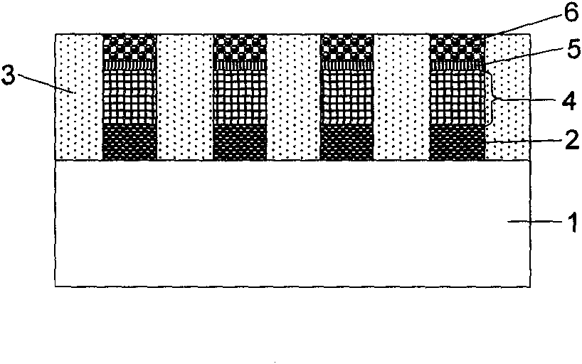
[0065] It has also been described in the above-mentioned embodiments, and in Figure 1A and Figure 1B In the structure, a bipolar transistor can be used instead of the PN diode 4 as the gating transistor. If a bipolar transistor is used as the gating tube, Figure 1D The PN layer 10 formed in the above method should be correspondingly changed into an NPN layer or a PNP layer, and the subsequent corresponding process is similar to that of the first embodiment. In the finally obtained multi-layer stacked resistive memory structure shown in FIG. 10 , the difference is that the gating units used in the layers 22-25 are bipolar transistors.

Embodiment 3

[0067] The difference between this embodiment and Embodiment 1 is that this embodiment is a method for manufacturing a Schottky diode-gated three-dimensional stacked resistive switching memory.

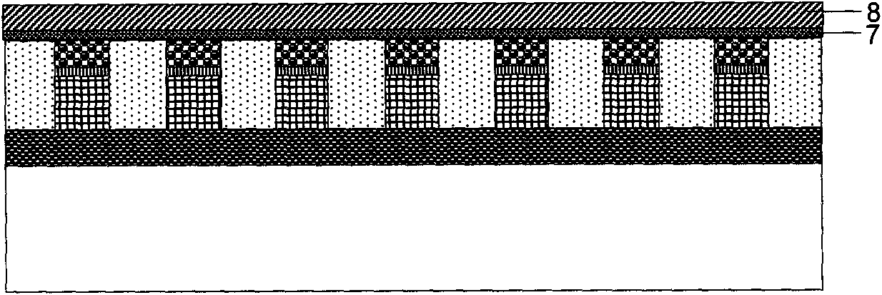
[0068] (1) Figure 2A What is shown is a substrate fabricated with peripheral circuits and a layer of resistive switch memory storage array, and the peripheral circuits are also not shown, but it does not mean that the substrate 31 does not have peripheral circuits. The gating tube used in this case is a Schottky diode. Of course, other gating units can also be used, such as PN diodes and bipolar transistors. Here, the Schottky diode is used as an example, but it is not necessary to explain limited to Schottky diodes. Multiple Schottky diodes 34 share one word line 32 , and the interface of the Schottky barrier formed by the Schottky diodes can be at the interface with the word line 32 or with the electrode 35 . The electrode 35 is also the heating electrode of the phase change memo...


PUM


Abstract

The invention provides a method for manufacturing a three-dimensionally stacked resistance conversion memory, which comprises the following steps of: sequentially depositing an adhesion layer and a metal layer on the surface provided with a peripheral circuit and a resistance converting storage array, and planing the surface under the assistance of chemically mechanical polishing to form a wafer 1 needing to be bonded; manufacturing a wafer 2 needed by bonding, namely, forming a PN layer on the wafer, activating the wafer, sequentially depositing an adhesion layer and a metal layer on the surface of the wafer, and planing the surface; bonding the wafer 1 and the wafer 2; and removing excessive part of the wafer 2 through subsequent processes, such as back etching, polishing or annealing and stripping process. The invention also includes the method for manufacturing the three-dimensionally stacked resistance conversion memory for manufacturing a schottky diode strobe. The method of the invention can make a process and a resistance conversion memory process compatible, has high reliability and fewer shortcomings, and is expected to be widely applied in three-dimensional stack.

Description

technical field [0001] The invention belongs to the field of semiconductor devices, and relates to a method for manufacturing a resistance switching memory, in particular to a method for manufacturing a three-dimensional stacked resistance switching memory, which is used in the manufacture of semiconductor devices. Background technique [0002] Multilayer stacking of semiconductor devices is an inevitable trend in the development of integrated circuits. Multilayer stacked semiconductor devices not only achieve a doubling of integration, but also increase the speed of the device. Within the appropriate number of layers, the device's Costs will also be significantly reduced, making semiconductor devices more competitive. [0003] Resistance switching memory such as phase change memory and resistance random access memory is the hottest next-generation non-volatile semiconductor memory today, with broad market prospects. Resistance switching memory has high storage density, simp...

Claims


Application Information

Patent Timeline
IPC IPC(8): H01L21/60H01L21/82H01L27/24
Inventor 张挺马晓波宋志棠刘旭焱刘波封松林
Owner SHANGHAI INST OF MICROSYSTEM & INFORMATION TECH CHINESE ACAD OF SCI
Why Eureka
Try Eureka