Method for measuring residual deformation of micro-nano metallic interconnect

A technology of metal interconnection and residual deformation, which is applied in the direction of measuring devices, instruments, and optical devices, etc., can solve the problems that it is difficult to be suitable for metal interconnection and micro-nano metal interconnection, and achieve simple operation, The effect of high measurement accuracy and accurate spatial positioning

Inactive Publication Date: 2010-09-22
TSINGHUA UNIV
View PDF0 Cites 18 Cited by
  • Summary
  • Abstract
  • Description
  • Claims
  • Application Information

AI Technical Summary

Problems solved by technology

[0003] The commonly used method for evaluating the internal residual stress of metal thin films including thin film wires is X-ray diffraction method. However, the applicable condition of this method is that the spot diameter of X-ray beam is smaller than the lateral and longitudinal dimensions of the object to be measured, while the current spot of X-ray beam can The minimum size achieved is 1 micron, and in actual o

Method used


Image

  • Method for measuring residual deformation of micro-nano metallic interconnect
  • Method for measuring residual deformation of micro-nano metallic interconnect
  • Method for measuring residual deformation of micro-nano metallic interconnect

Examples


Embodiment 1

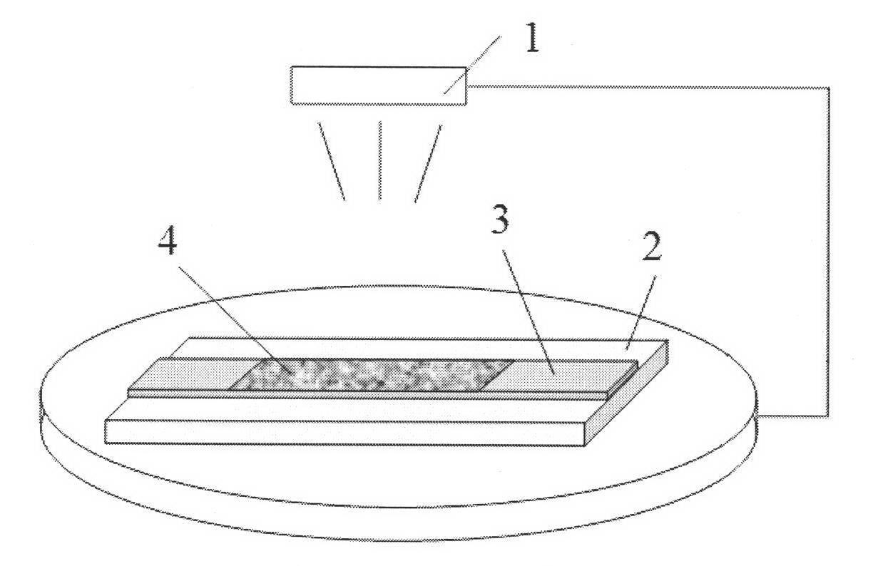
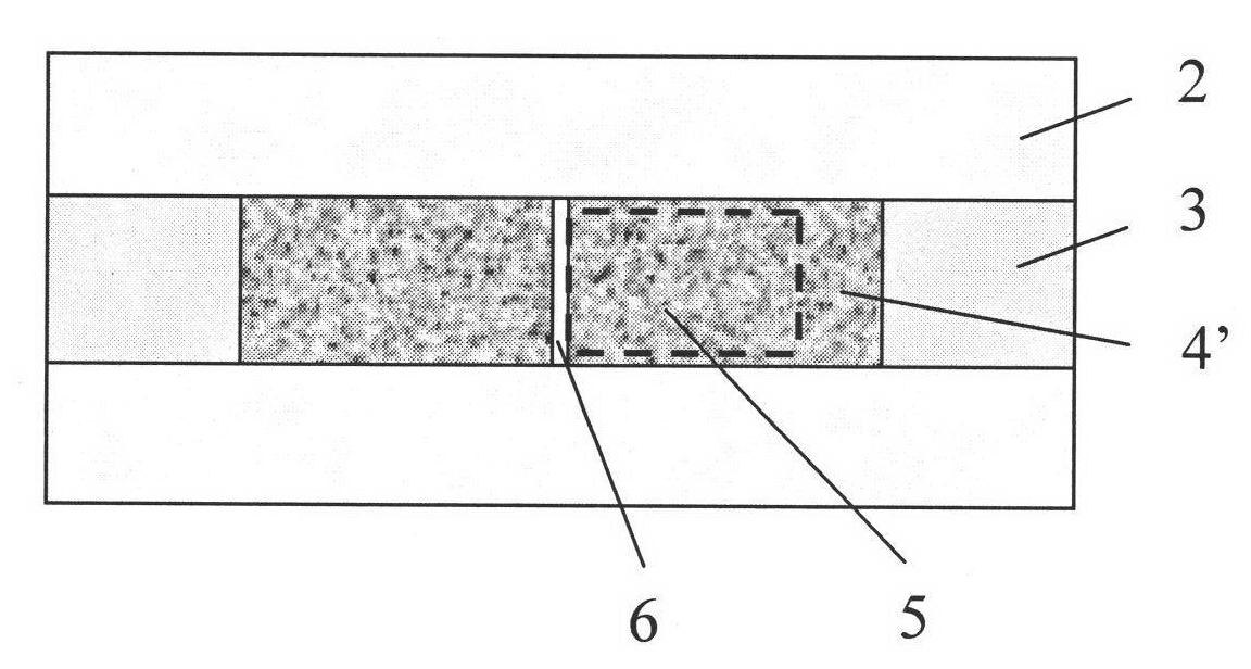
[0034] In this embodiment, speckle is used as a micro-marker. It is intended to measure the residual deformation of the copper interconnection due to the release of residual stress. The copper interconnection is deposited on a silicon substrate. The width and thickness of the copper interconnection are 20 μm and 300 nm, respectively. The distance between the centers of two adjacent copper interconnection lines is 40 μm, and the length of the copper interconnection lines is 3 mm. Place the copper interconnect sample deposited on the silicon substrate on the platform of the focused ion beam system, and select a region of a copper interconnect as the research object.

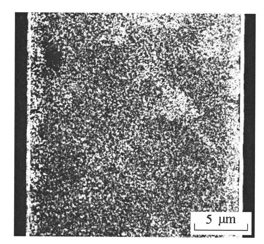
[0035] Use the ion beam in the focused ion beam system to irradiate the copper interconnection line, stop the irradiation when the speckle is clearly visible, and collect the speckle image on the copper interconnection line at this time as the micromarker image before the axial residual stress is released , the siz...


PUM

PropertyMeasurementUnit
Crack widthaaaaaaaaaa

Abstract

The invention discloses a method for measuring residual deformation of micro-nano metallic interconnect, belonging to the fields of deformation survey and optical measurement mechanics. The method includes the following steps: fabricating speckles on the surface of the micro-nano metallic interconnect through irradiation by focused ion beams or etching a unidirectional grating through the focused ion beams to be used as the micro-nano mark; then etching a through crack vertical to the axis in the micro-nano mark area through the focused ion beams so as to release the axial residual stress; respectively collecting the micro-nano mark images before and after the crack is etched; calculating the deformation, i.e. the residual deformation of the micro-nano metallic interconnect close to the crack caused by the residual stress by using digital image correlation method. Through the method, micro-nano mark can be fabricated in situ, crack can be etched and images can be collected, and the method has the advantages of in situ measurement, precise positioning, simple operation, non contact, simple data processing, high sensitivity and high measurement precision. Through the method of irradiation by focused ion beams, speckles can be fabricated quickly and the process is simple and convenient.

Description

technical field [0001] The invention relates to a method for measuring the residual deformation of micro-nano metal interconnection wires, belonging to the fields of deformation measurement and optical measurement mechanics. Background technique [0002] Metal interconnects are widely found in semiconductor integrated circuits and micro-electromechanical systems. With the increasing performance requirements for micro-devices, the width of metal interconnects is also getting smaller and smaller, ranging from tens of microns to tens of nanometers. Due to the difference in thermal expansion coefficient between the micro-nano metal interconnection, the substrate, and the insulating layer, the pre-stress that is difficult to eliminate will be generated during the preparation process of the micro-nano metal interconnection, which is called residual stress. This pre-existing residual stress is likely to cause electromigration of the micro-nano metal interconnection during use. If t...

Claims


Application Information

Patent Timeline
IPC IPC(8): G01B11/16
Inventor 谢惠民王庆华徐可为王剑锋
Owner TSINGHUA UNIV
Why Eureka
Try Eureka