Silicon controlled rectifier electro-static discharge protective circuit structure triggered by diode

A technology for protecting circuits and electrostatic discharge, which is applied in the electronic field and can solve problems such as unfavorable protection of internal circuit devices

Inactive Publication Date: 2010-09-22
UNIV OF ELECTRONICS SCI & TECH OF CHINA
View PDF3 Cites 19 Cited by
  • Summary
  • Abstract
  • Description
  • Claims
  • Application Information

AI Technical Summary

Problems solved by technology

for figure 1 For the SCR structure shown, to increase its sustain voltage, it is necessary to increase the P well package cathode N + or N well package anode P + The ...

Method used


Image

  • Silicon controlled rectifier electro-static discharge protective circuit structure triggered by diode
  • Silicon controlled rectifier electro-static discharge protective circuit structure triggered by diode
  • Silicon controlled rectifier electro-static discharge protective circuit structure triggered by diode

Examples


specific Embodiment approach 1

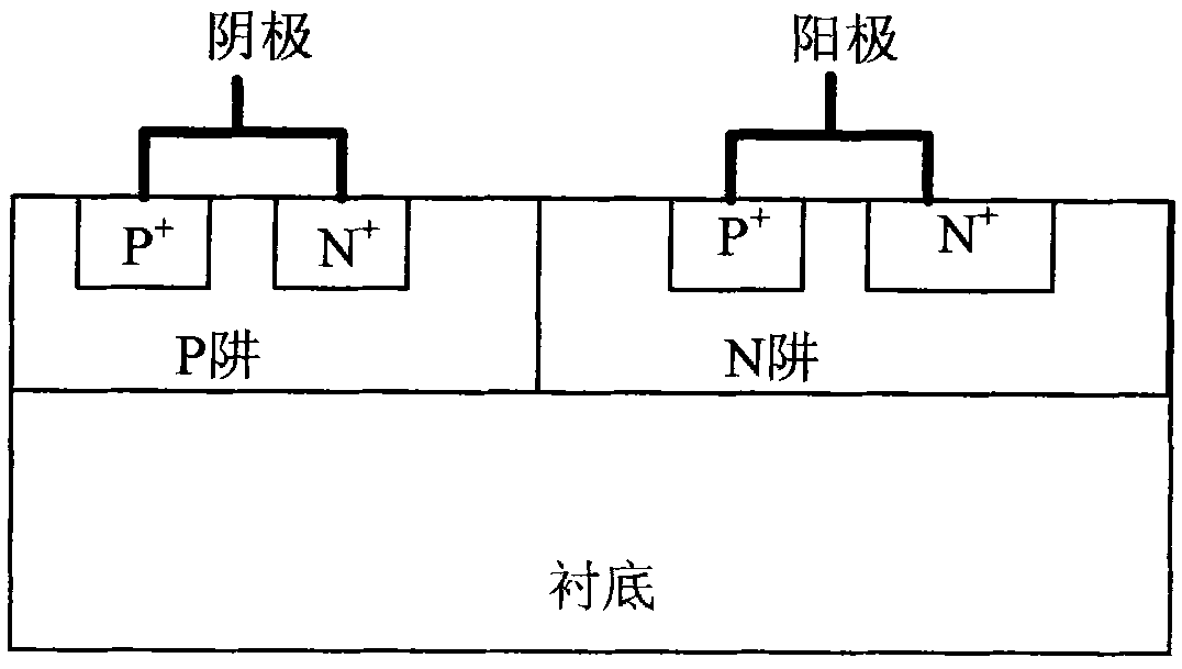
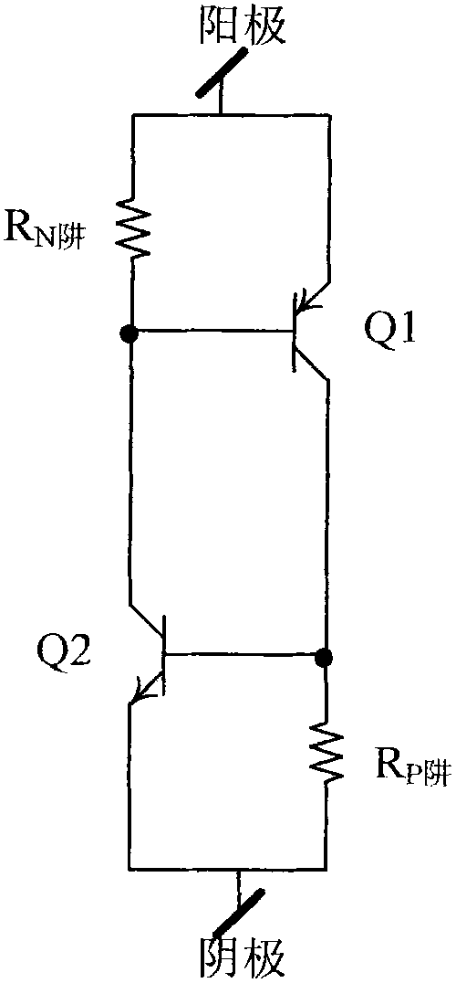
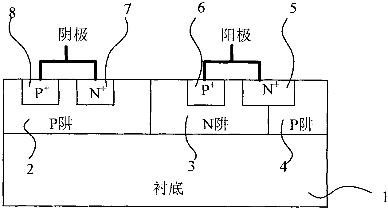
[0024] A diode-triggered thyristor rectifier electrostatic discharge protection circuit structure, such as image 3 As shown, it includes: two conductivity types of well regions located on the semiconductor substrate substrate 1: P-type well region 2 and N-type well region 3; two heavily doped well regions located in the first P-type well region 2 District: P + heavily doped region 8 and N + Heavily doped region 7; two heavily doped regions located in N-type well region 3: P + heavily doped region 6 and N + The heavily doped region 5 ; the cathode contacting the surfaces of the two heavily doped regions in the first P-type well region 2 ; the anode contacting the surfaces of the two heavily doped regions in the N-type well region 3 . The protection circuit structure also includes a second P-type well region 4, the second P-type well region 4 is connected to the first P-type well region 2 and surrounds the N-type well region 3 in the middle, and the N-type well region N in ...

specific Embodiment approach 2

[0028] A diode-triggered thyristor rectifier electrostatic discharge protection circuit structure, such as Figure 5 As shown, it includes: two conductivity types of well regions located on the semiconductor substrate substrate 1: N-type well region 2 and P-type well region 3; two heavily doped well regions located in the first N-type well region 2 District: N + Zone 8 and P + Open region 7; two heavily doped regions located in the P-type well region 3: N + Zone 6 and P + Region 5; an anode in contact with the surfaces of the two heavily doped regions in the first N-type well region 2; a cathode in contact with the surfaces of the two heavily doped regions in the P-type well region 3. The protection circuit structure also includes a second N-type well region 4, the second N-type well region 4 is connected to the first N-type well region 2 and surrounds the P-type well region 3 in the middle, and the P-type well region P in zone 3 + A part of the region 5 is located in the...

specific Embodiment approach 3

[0032] Such as Figure 8 As shown, on the basis of the technical solution of Embodiment 1, a P well not connected to the existing two heavily doped regions is added in the first P-type well region 2. + Heavily doped region 9, while adding a P well not connected to the existing heavily doped region in the second P-type well region 4 + heavily doped region 10; and the two increased P + The heavily doped regions 9 and 10 are interconnected by metal wires.

[0033] When adding two P + After the heavily doped regions 9 and 10, in the case of parasitic diode breakdown, the hole current is mainly composed of P + Heavily doped region 10, and flows to P through the wire + The heavily doped region 9 flows through the P-type well region 2 to the N in the P-type well region 2 + The heavily doped region 7 is finally collected by the cathode electrode. This can make the hole current distribution more uniform, so as to form a uniform voltage drop on the P well, so as to avoid the inhom...


PUM


Abstract

The invention relates to a silicon controlled rectifier (SCR) electro-static discharge (ESD) protective circuit structure triggered by a diode, which belongs to the technical field of the electron. The invention converts a trigger voltage of a conventional SCR ESD protective circuit structure into a N+/P-well (or N-well/P+) junction breakdown voltage from a P-well/N-well junction breakdown voltage by integrating the diode with lower breakdown voltage so as to reduce the trigger voltage of the SCR ESD protective circuit structure and finally play a role of well protecting an internal circuit of a chip. Meanwhile, under the premise of not changing the trigger voltage, the silicon controlled rectifier (SCR) electro-static discharge (ESD) protective circuit structure can obtain an adjustable device maintaining voltage by simply adjusting size parameters of devices. The invention is compatible with a CMOS process, also can adopt processes of BiCMOS, BCD, SOI and the like, can connect the protective circuit structure provided by the invention between a power of an integrated circuit and the ground to serve as the ESD protection of a Power Clamp and also can connect the protective circuit structure among an input port and an output port of the integrated circuit and the power (the ground) to serve as the ESD protection of the input port and the output port.

Description

technical field [0001] The invention belongs to the field of electronic technology, and relates to a protection circuit for electrostatic discharge (ESD for short) in an integrated circuit, in particular to a silicon controlled rectifier (Semiconductor Controlled Rectifier, SCR for short) electrostatic discharge circuit structure. Background technique [0002] Electrostatic discharge is a common phenomenon in the process of manufacturing, producing, assembling, testing, storing, and transporting semiconductor devices or circuits. The excess charge it brings will pass through the I The / O pin is passed into the integrated circuit and destroys the internal circuit of the integrated circuit. In order to solve this problem, manufacturers usually set up a protection circuit between the internal circuit and the I / O pin. This protection circuit must be activated before the pulse current of electrostatic discharge reaches the internal circuit to quickly eliminate the excessive volta...

Claims


Application Information

Patent Timeline
IPC IPC(8): H01L27/06H01L29/74H01L29/06
CPCH01L29/87H01L29/0692H01L29/0649
Inventor 蒋苓利张波樊航乔明刘娟韩山明钟昌贤
Owner UNIV OF ELECTRONICS SCI & TECH OF CHINA
Why Eureka
Try Eureka