

Piezoelectric film bulk acoustic wave sensor with polygonal electrodes
A thin-film bulk acoustic wave and piezoelectric thin-film technology, applied in piezoelectric devices/electrostrictive devices, piezoelectric/electrostrictive/magnetostrictive devices, using sound waves/ultrasonic waves/infrasonic waves to analyze fluids, etc., can solve production costs Improvement, complex device processing technology, complex electrode shape and other problems, to achieve the effect of simple structure
- Summary
- Abstract
- Description
- Claims
- Application Information
AI Technical Summary
Problems solved by technology
Method used
Image

Examples
Embodiment 1
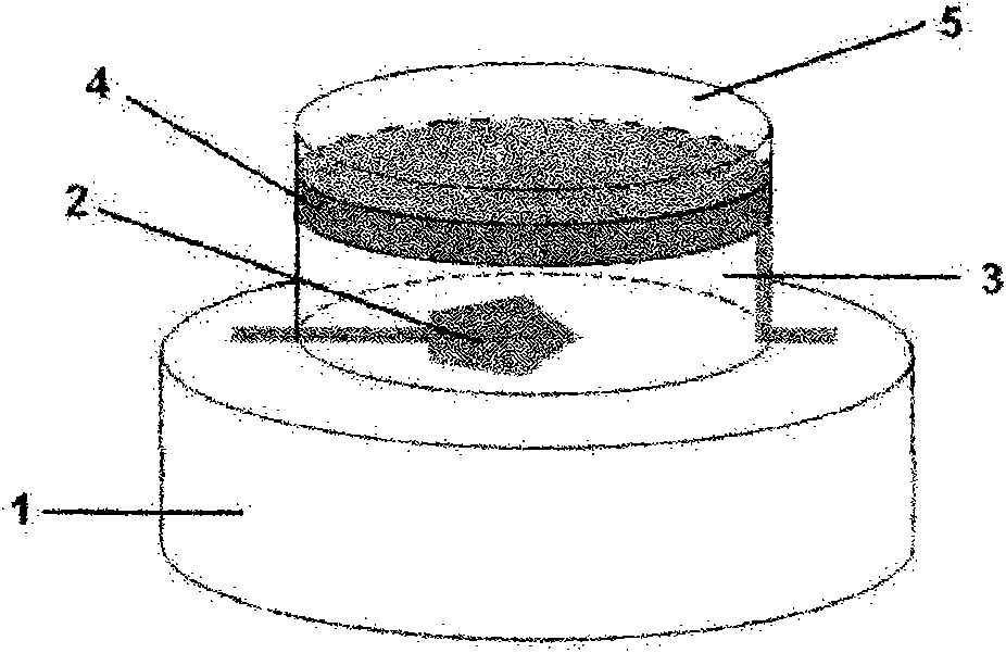
[0025] Piezoelectric film bulk acoustic wave sensors with single-sided pentagonal electrodes and single-sided all-metal electrodes.
[0026] 1. Select a p-type (100) crystal-oriented Si substrate (1), and wash it with acetone, absolute ethanol and deionized water in sequence;
[0027] 2. Deposit the metal lower electrode (2), and form the pentagonal metal lower electrode by photolithography and etching;
[0028] 3. Using the magnetron sputtering method, using high-purity Al as the target material, Ar and N 2 Depositing an AlN piezoelectric thin film (3) with a preferred orientation parallel to the c-axis for the reaction gas, and photoetching and etching the AlN film layer to expose the leads of the pentagonal metal lower electrode;
[0029] 4. Deposit a single-sided all-metal upper electrode (4) covering the upper surface of the AlN film, and lead the upper electrode to the lower surface of the AlN film to connect to the external circuit;
[0030] 5. Deposit a layer of sens...
Embodiment 2
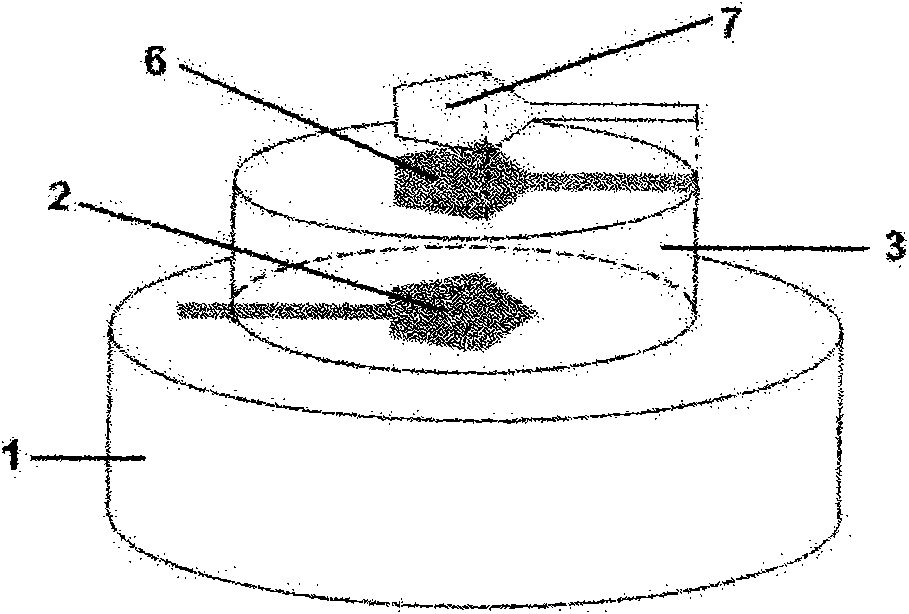
[0032] Piezoelectric film bulk acoustic wave sensor with double-sided pentagonal metal electrodes.
[0033] 1. Select a p-type (100) crystal-oriented Si substrate (1), and wash it with acetone, absolute ethanol and deionized water in sequence;
[0034] 2. Deposit the pentagonal metal lower electrode (2), and form the pentagonal metal lower electrode by photolithography and etching;
[0035] 3. Using the magnetron sputtering method, using high-purity Al as the target material, Ar and N 2 Depositing an AlN piezoelectric thin film (3) with a preferred orientation parallel to the c-axis for the reaction gas, and photoetching and etching the AlN film layer to expose the leads of the pentagonal metal lower electrode;
[0036] 4. Deposit a pentagonal metal upper electrode (6), and form a pentagonal metal upper electrode by photolithography and etching;
[0037] 5. Deposit the sensitive film Au(7), and form a sensitive film with the same shape and area as the pentagonal metal upper ...
Embodiment 3
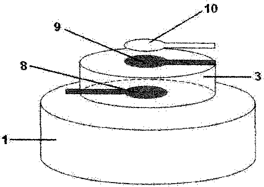
[0039] Piezoelectric film bulk acoustic wave sensor with double-sided circular metal electrodes.
[0040] 1. Select a p-type (100) crystal-oriented Si substrate (1), and wash it with acetone, absolute ethanol and deionized water in sequence;
[0041] 2. Deposit a circular metal lower electrode (8), and form a circular metal lower electrode by photolithography and etching;
[0042] 3. Using the magnetron sputtering method, using high-purity Al as the target material, Ar and N 2 Depositing an AlN piezoelectric film (3) with a preferred orientation parallel to the c-axis for the reaction gas, and photolithography and etching the AlN film layer to expose the lead of the circular metal lower electrode;
[0043] 4. Deposit a circular metal upper electrode (9), and form a circular metal upper electrode by photolithography and etching;
[0044] 5. Deposit a sensitive film of Au(10), and form a sensitive film with the same shape and area as the circular metal upper electrode by photo...
PUM
 Abstract
Description
Claims
Application Information