GaN-based LED epitaxial wafer and growing method thereof
An LED epitaxial wafer, GaN-based technology, applied in gaseous chemical plating, coating, electrical components, etc., can solve the problem that the antistatic ability of GaN-based LED chips is limited, and the dislocation of GaN-based epitaxial layers is not greatly reduced. Density and stress, etc., to achieve the effect of reducing dislocation density and improving working life
- Summary
- Abstract
- Description
- Claims
- Application Information
AI Technical Summary
Problems solved by technology
Method used
Image

Examples
Embodiment 1
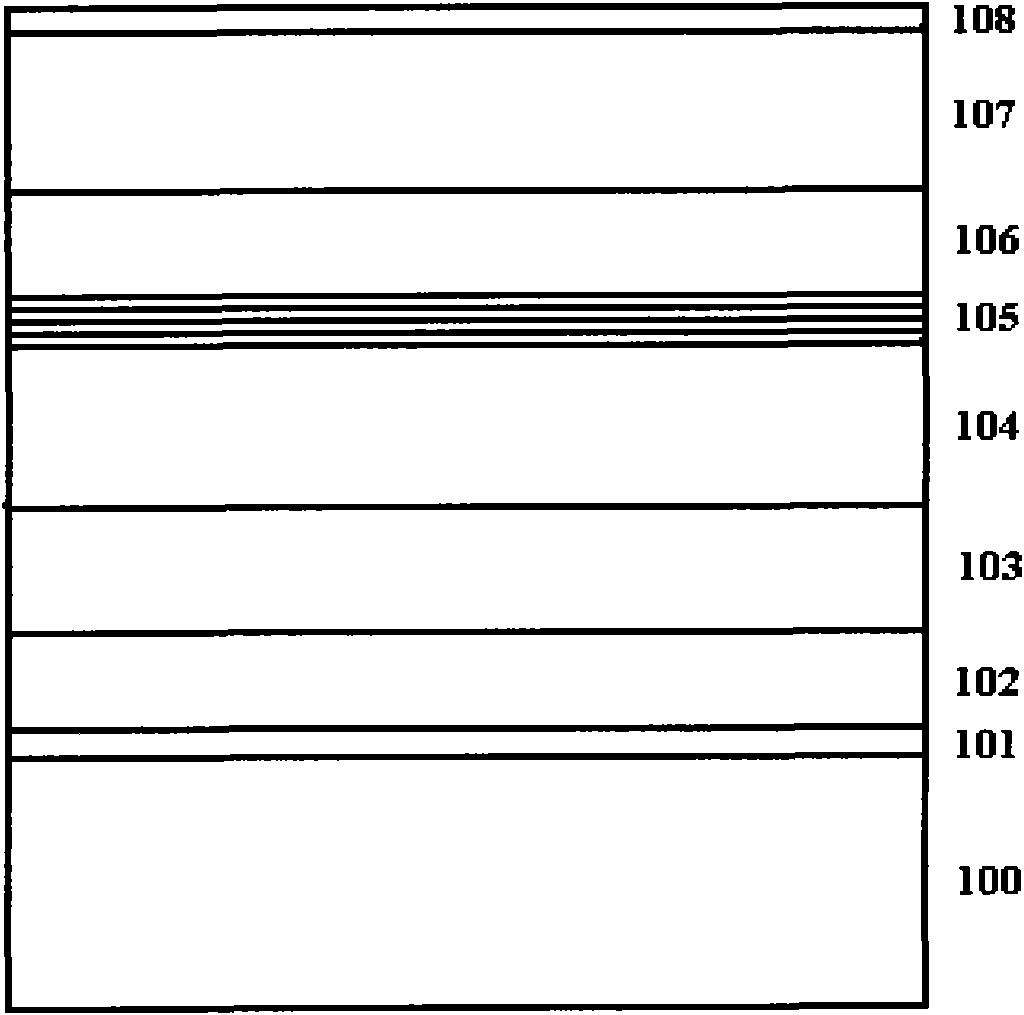
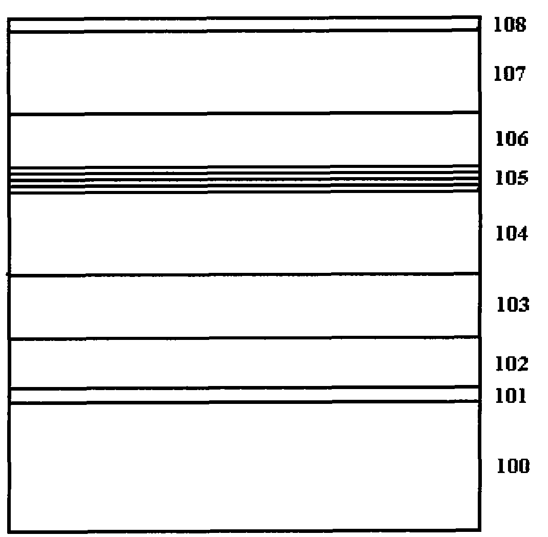
[0024] Embodiment 1 Using MOCVD to grow epitaxial wafers, grow sequentially from bottom to top:
[0025] 1. Put the sapphire substrate with (0001) crystal orientation into the reaction chamber, and then 2 The temperature in the environment is raised to 1050° C., stabilized for 10 minutes, and the substrate is purified at high temperature.
[0026] 2. Lower the temperature to 530° C. to grow a low-temperature GaN-based buffer layer with a thickness of 20 nm.
[0027] 3. Raise the temperature to 1100° C., keep the pressure at 500 Torr, and grow a first non-doped GaN layer with a thickness of 500 nm.
[0028]4. At 1100° C., a second non-doped GaN layer with a thickness of 1.5 μm is grown at a reduced pressure of 300 Torr.
[0029] 5. An n-type GaN layer with a thickness of 1.5 μm is grown at 1100° C.
[0030] 6. In N 2 The multi-quantum well layer is grown for 5 periods in the environment, the GaN barrier layer: the thickness is 20nm, the growth temperature is 850°C; the InGa...
Embodiment 2
[0036] Embodiment 2 Using MOCVD to grow epitaxial wafers, grow sequentially from bottom to top:
[0037] 1. Put the sapphire substrate with (0001) crystal orientation into the reaction chamber, and then 2 The temperature in the environment is raised to 1250° C., stabilized for 5 minutes, and the substrate is purified at high temperature.
[0038] 2. Lower the temperature to 540° C. to grow a low-temperature GaN-based buffer layer with a thickness of 30 nm.
[0039] 3. Raise the temperature to 1200° C. and increase the pressure to 400 Torr to grow a first non-doped GaN layer with a thickness of 400 nm.
[0040] 4. At 1200° C., reduce the pressure to 200 Torr to grow a second non-doped GaN layer with a thickness of 1.6 μm.
[0041] 5. Grow n-type GaN with a thickness of 2 μm at 1200°C.
[0042] 6. In N 2 The multi-quantum well layer is grown for 15 cycles in the environment, the GaN barrier layer: the thickness is 13nm, the growth temperature is 950°C; the InGaN well layer: ...
Embodiment 3
[0049] Embodiment 3 Using MOCVD to grow epitaxial wafers, grow sequentially from bottom to top:
[0050] 1. Put the sapphire substrate with (0001) crystal orientation into the reaction chamber, and then 2 The temperature in the environment is raised to 1150° C., stabilized for 7 minutes, and the substrate is purified at high temperature.
[0051] 2. Lower the temperature to 550° C. to grow a low-temperature GaN-based buffer layer with a thickness of 25 nm.
[0052] 3. Raise the temperature to 1180° C. and increase the pressure to 300 Torr to grow a first non-doped GaN layer with a thickness of 50 nm.
[0053] 4. At 1180° C., reduce the pressure to 150 Torr to grow a second non-doped GaN layer with a thickness of 1.95 μm.
[0054] 5. A 3 μm thick n-type GaN layer was grown at 1180° C.
[0055] 6. In N 2 The multi-quantum well layer is grown for 10 periods in the environment, the GaN barrier layer: the thickness is 15nm, the growth temperature is 850°C; the InGaN well layer:...
PUM
| Property | Measurement | Unit |
|---|---|---|
| Thickness | aaaaa | aaaaa |
| Thickness | aaaaa | aaaaa |
| Thickness | aaaaa | aaaaa |
Abstract
Description
Claims
Application Information
 - R&D
- Intellectual Property
- Life Sciences
- Materials
- Tech Scout
- Unparalleled Data Quality
- Higher Quality Content
- 60% Fewer Hallucinations
Browse by: Latest US Patents, China's latest patents, Technical Efficacy Thesaurus, Application Domain, Technology Topic, Popular Technical Reports.
© 2025 PatSnap. All rights reserved.Legal|Privacy policy|Modern Slavery Act Transparency Statement|Sitemap|About US| Contact US: help@patsnap.com