Light trapping structure for thin film silicon/crystalline silicon heterojunction solar battery

A light trapping structure and solar cell technology, applied in the field of light trapping structure, can solve the problems of difficulty in obtaining high-performance thin-film silicon/crystalline silicon heterojunction solar cells, increasing the difficulty of the heterojunction interface, and reduce the interface state density. The effect of good solar cell performance and high performance

Inactive Publication Date: 2010-10-20
INST OF ELECTRICAL ENG CHINESE ACAD OF SCI
View PDF7 Cites 32 Cited by
  • Summary
  • Abstract
  • Description
  • Claims
  • Application Information

AI Technical Summary

Problems solved by technology

In particular, in order to obtain an excellent light-trapping effect for ordinary solar cells, it is necessary to weave the surface of the crystalline silicon substrate. For example, use an alkaline etching solution to etch a pyramid structure on the surface of the silicon wafer. With a higher density of defect states, the difficulty of passivating the heterojunction interface is further increased
This is the main reason why it is difficult for many research institutions to obtain high-performance thin-film silicon / crystalline silicon heterojunction solar cells

Method used


Image

  • Light trapping structure for thin film silicon/crystalline silicon heterojunction solar battery
  • Light trapping structure for thin film silicon/crystalline silicon heterojunction solar battery
  • Light trapping structure for thin film silicon/crystalline silicon heterojunction solar battery

Examples


Embodiment 1

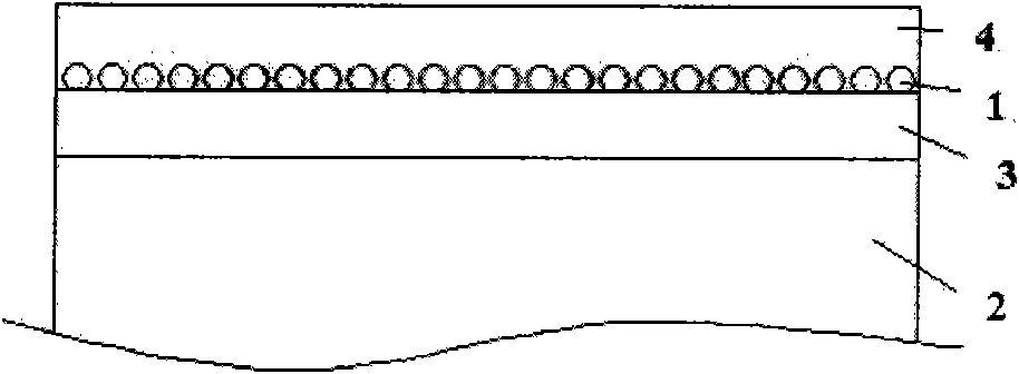
[0037] as attached figure 2 A light-trapping structure for thin-film silicon / crystalline silicon heterojunction solar cells shown, the light-trapping structure includes: a crystalline silicon substrate (2), on the light-facing surface of the crystalline silicon substrate (2) The doped thin film silicon layer (3), the metal nanostructure (1) on the doped thin film silicon layer (3), and the transparent conductive electrode (4) on the metal nanostructure (1); wherein , the light-facing surface of the crystalline silicon substrate (2) is not intentionally woven, and the metal nanostructure (1) is metal nanoparticles.

Embodiment 2

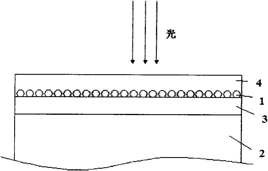
[0039] as attached image 3 A light-trapping structure for thin-film silicon / crystalline silicon heterojunction solar cells shown, the light-trapping structure includes: a crystalline silicon substrate (2), on the light-facing surface of the crystalline silicon substrate (2) The doped thin film silicon layer (3), the transparent conductive electrode (4) on the doped thin film silicon layer (3), and the metal nanostructure (1) on the transparent conductive electrode (4); wherein , the light-facing surface of the crystalline silicon substrate (2) is not intentionally woven, and the metal nanostructure (1) is a metal nanospace network.

Embodiment 3

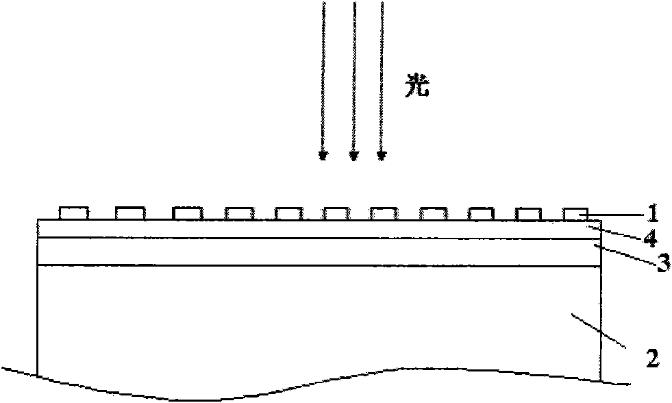
[0041] as attached Figure 4A light-trapping structure for thin-film silicon / crystalline silicon heterojunction solar cells is shown, the light-trapping structure includes: a crystalline silicon substrate (2), on the backlight surface of the crystalline silicon substrate (2) A doped thin film silicon layer (3), a transparent conductive electrode (4) on the doped thin film silicon layer (3), and a metal nanostructure (1) inside the transparent conductive electrode (4); wherein, The backlight surface of the crystalline silicon substrate (2) is not intentionally woven, and the metal nanostructure (1) is a metal nanodisk.


PUM


Abstract

The invention discloses a light trapping structure for a thin film silicon/crystalline silicon heterojunction solar battery, which comprises a crystalline silicon substrate (2), a doped thin film silicon layer (3) on the crystalline silicon substrate (2), a transparent conductive electrode (4) on the doped thin film silicon layer (3), and a metal nano-structure (1) between the doped thin film silicon layer (3) and the transparent conductive electrode (4), a metal nano-structure (1) above the transparent conductive electrode (4), or a metal nano-structure (1) inside the transparent conductive electrode (4). The connecting surface of the crystalline silicon substrate (2) and the crystalline silicon substrate (2) is not specially woven with velvet. The light trapping structure acquires a light trapping effect by using a surface plasmon effect of the metal nano-structure.

Description

technical field [0001] The invention relates to a light-trapping structure for thin-film silicon / crystalline silicon heterojunction solar cells, in particular to a light-trapping structure for thin-film silicon / crystalline silicon heterojunctions using the surface plasmon effect of metal nanostructures Light-trapping structure of solar cells. Background technique [0002] Thin-film silicon / crystalline silicon heterojunction solar cells are high-efficiency crystalline silicon solar cells that can be realized at low cost. This kind of solar cell uses a doped thin film silicon layer to make a pn junction on a crystalline silicon substrate. This layer of thin-film silicon layer is usually only a dozen nanometers thick, and can be deposited below 200°C by plasma-assisted chemical vapor deposition (PECVD). Therefore, compared with traditional solar cells that rely on diffusion to prepare pn junctions , Thin-film silicon / crystalline silicon heterojunction solar cells require less...

Claims


Application Information

Patent Timeline
Patent Type & Authority Applications(China)
IPC IPC(8): H01L31/0392H01L31/0224
CPCY02E10/50
Inventor 赵雷王文静
Owner INST OF ELECTRICAL ENG CHINESE ACAD OF SCI
Why Eureka
Try Eureka