Novel semiconductor light-emitting diode

A technology of light-emitting diodes and semiconductors, applied in the direction of semiconductor devices, electrical components, circuits, etc., can solve the problems of reduced electrode reliability, current congestion of LED devices, and reduced light output, so as to enhance lateral current diffusion, eradicate shading effects, and avoid The effect of heat concentration

Inactive Publication Date: 2010-10-20
常州美镓伟业光电科技有限公司 +1
View PDF4 Cites 41 Cited by
  • Summary
  • Abstract
  • Description
  • Claims
  • Application Information

AI Technical Summary

Problems solved by technology

[0005] In order to overcome the defects of existing LED devices, the present invention provides a new semiconductor light-emitting diode with uniform light output, high luminous efficiency and reliable ele

Method used


Image

  • Novel semiconductor light-emitting diode
  • Novel semiconductor light-emitting diode
  • Novel semiconductor light-emitting diode

Examples


Embodiment Construction

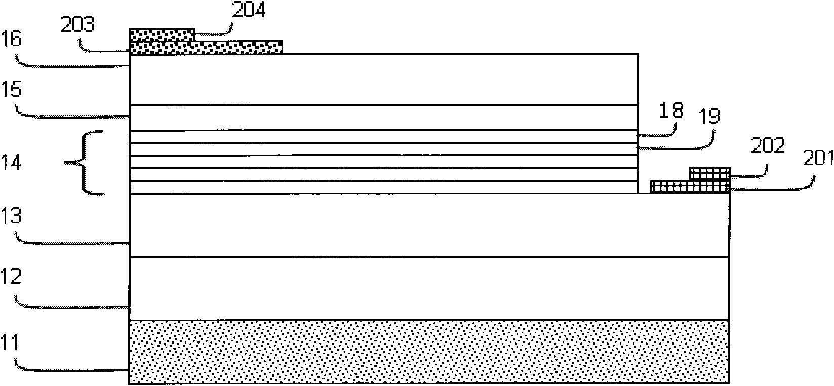
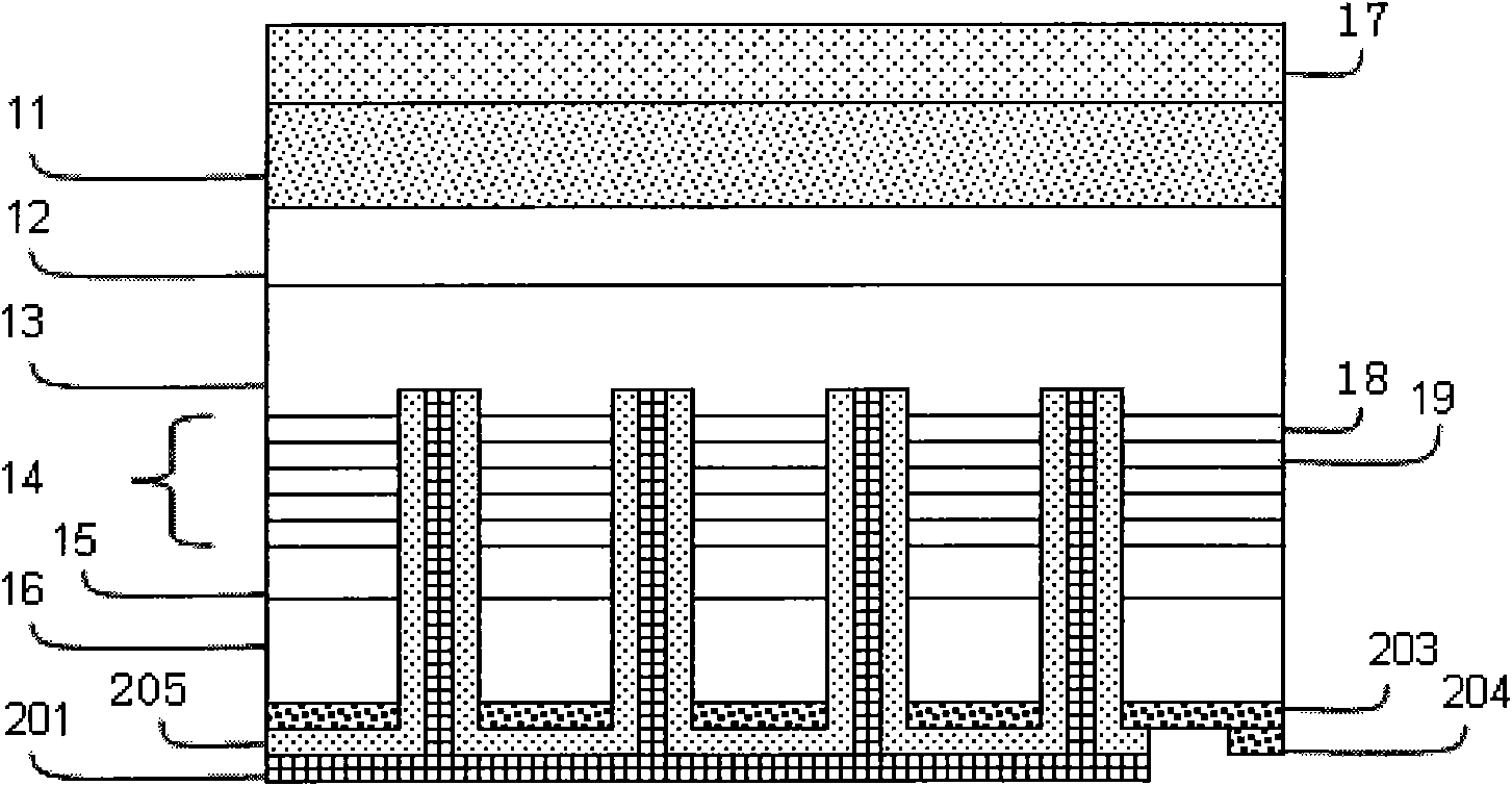
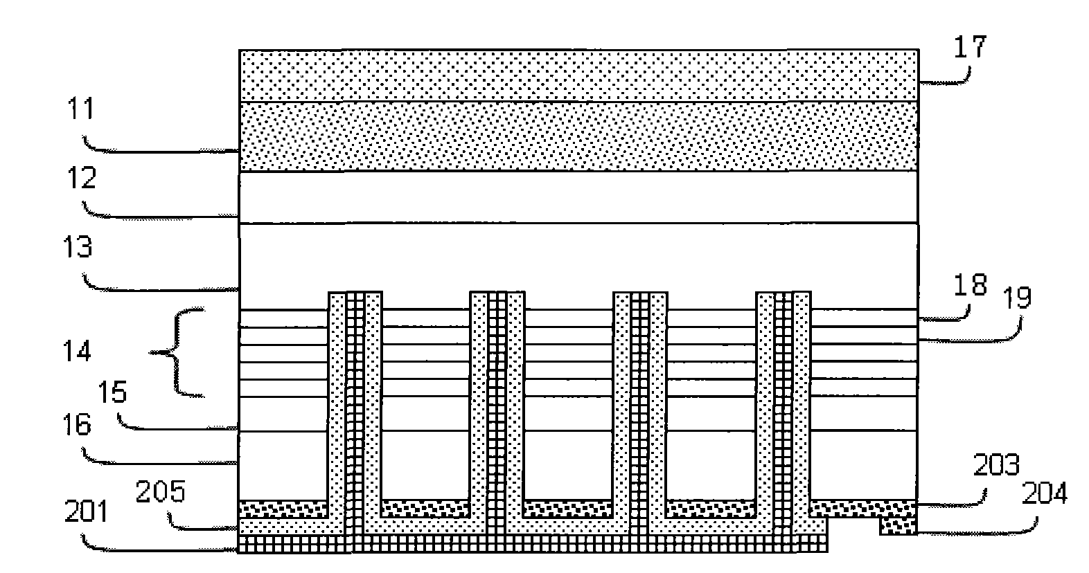
[0018] Such as figure 2 Shown: the present invention relates to a novel semiconductor light-emitting diode, comprising sequentially compounded phosphor layer 17, substrate 11, buffer layer 12, N-type layer 12, active layer 14, with a selected thickness of 10 nanometers, 100 nanometers or 200 nanometers Nanometer electron blocking layer 15, P-type layer 16 with a thickness of 10 nanometers, 1 micron or 8 microns, P-type contact metal layer 203, P-type contact metal layer 203 and N-type contact metal layer 201 separated by insulating layer 205 Etching is performed locally on the surface of the P-type layer 16 of the LED device to form three grooves, which respectively penetrate the P-type layer 16, the active layer 14 and part of the N-type layer 13, thereby exposing the surface of the N-type layer 13 material On the side of the P-type material, the gallium nitride-based material of the N-type layer is In x Al y Ga 1-x-y N(0≤x≤1, 0≤y≤1, 0≤x+y≤1), and the ratio of x and y can...


PUM

PropertyMeasurementUnit
Single layer thicknessaaaaaaaaaa
Thicknessaaaaaaaaaa
Thicknessaaaaaaaaaa

Abstract

The invention relates to a novel semiconductor light-emitting diode, which comprises a substrate, a buffer layer, an N-type layer, an active layer, an electronic barrier layer, a P-type layer and a P-type contact metal layer. The P-type layer, the electronic barrier layer, the active layer and the like are penetrated through etching; an N-type layer material is exposed to one side of a P-type material directly, and an N-type contact metal and an electrode are covered on an exposed area, so that the diffusion of transverse current in the N-type layer is enhanced; and simultaneously, a P-type metal covers an integral P-type semiconductor layer, and an LED emits light from the bottom surface of the substrate. Through the improvement, the transverse diffusion distance of the current in LED devices is shortened substantially, uneven distribution of current density in the LED devices due to current congestion is prevented, so that the LED devices emit the light uniformly, and the shading effect of a P-type electrode is eliminated.

Description

technical field [0001] The invention relates to a semiconductor light emitting diode. Background technique [0002] Semiconductor light emitting diode (Light Emitting Diode, hereinafter referred to as LED) is a semiconductor light emitting device, which uses gallium nitride series compound light emitting materials to cause photon recombination under forward voltage to emit light. LED directly emits white and various colored lights, and its luminous process includes carrier injection under forward bias voltage, recombined radiative luminescence and effective extraction of light energy. [0003] However, the current mainstream LED design adopts a Mesa-etch structure in which the N-type and P-type electrodes are located at the left and right ends of the LED, and its electron injection and diffusion are limited, resulting in reduced LED luminous efficiency and low luminous brightness. Uniform (such as figure 1 shown). Under high current density injection conditions, the area ...

Claims


Application Information

Patent Timeline
IPC IPC(8): H01L33/38
Inventor 廖翊韬云峰
Owner 常州美镓伟业光电科技有限公司
Why Eureka
Try Eureka