Method for preparing crystal silicon wafer cutting edge material

A cutting edge, crystalline silicon wafer technology, applied in the field of cutting and grinding materials, can solve the problems of low output, high water consumption, long pickling time, etc. Strong abrasive effect

Inactive Publication Date: 2011-05-25
HENAN XINDAXIN SCI & TECH
View PDF2 Cites 0 Cited by
  • Summary
  • Abstract
  • Description
  • Claims
  • Application Information

AI Technical Summary

Problems solved by technology

In recent years, my country's cutting edge production technology has made some progress. For example, Chinese patent document CN 100360400C discloses a method for preparing special cutting edge material for semiconductor material wire cutting from high-purity 6H-SiC. The production process, the products produced are more than 90% equal-area shape, and the yield is high, but the overall output of the jet mill is low, the shape of the produced particles is round, the sharpness is poor, and there are hidden cracks, not It is beneficial to cutting; in the prior art, Raymond mill is also used for crushing. Although the output of Raymond mill is high, the yield is low, and the output product is less in equal area, accounting for about 50%, and needle-shaped, flake-shaped, etc. There are many particles in the shape, the cutting efficiency is poor, and it is not wear-resistant; in the prior art, there are still traditional wet ball mills for crushing. Although the products have many equal-area shapes and good sharpness, the output is low and the yield is low. Over-grinding Serious; in addition, some existing cutting edge preparation processes still have shortcomings such as too long pickling time and high water consumption.

Method used


Image

  • Method for preparing crystal silicon wafer cutting edge material
  • Method for preparing crystal silicon wafer cutting edge material
  • Method for preparing crystal silicon wafer cutting edge material

Examples


Embodiment 1

[0027] Embodiment 1 A kind of preparation method of crystalline silicon wafer cutting blade comprises the following steps:

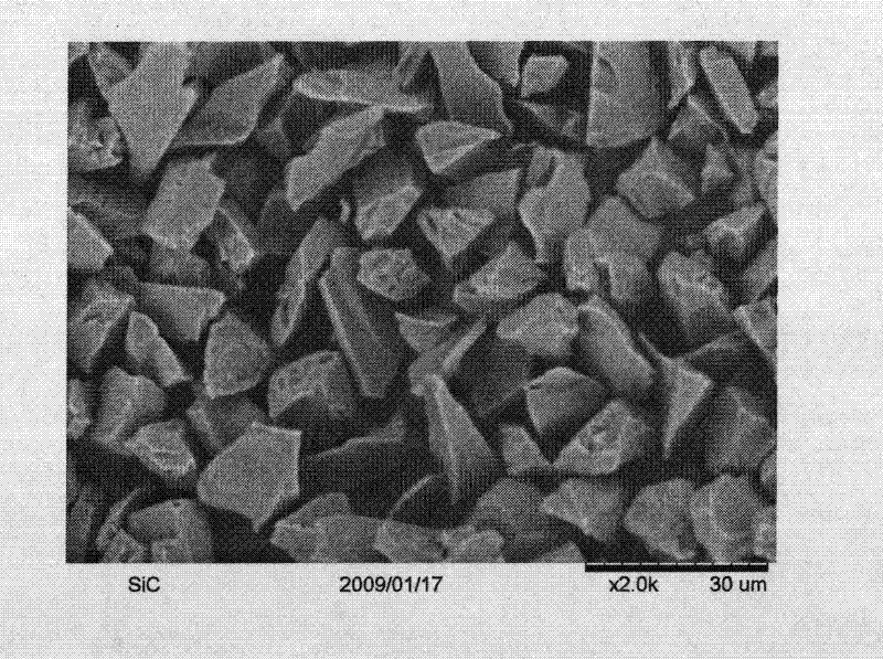
[0028] (1) Crushing of raw materials: select green silicon carbide block materials with a purity ≥ 98%, carry out jaw crushing and sieving, and collect silicon carbide particle size sand with a particle size ≤ 5mm;

[0029] (2) Dry ball mill classification: When using dry ball mill classifiers to grind the above-mentioned silicon carbide particle size sand, the amount of steel balls added is 400kg, the ball-to-material ratio is 3:1, the mill speed is 120rpm, and the primary airflow The speed of the classifier is 800rpm to obtain the main product (silicon carbide powder with a required particle size range of 4.5-18um), the speed of the secondary air classifier is 1800rpm to obtain by-products, and the air intake of the induced draft fan is 3000m 3 / h. Control the air intake of the induced draft fan, so that the fine powder that meets the particle size re...

Embodiment 2

[0037] Embodiment 2 A method for preparing a crystalline silicon wafer cutting blade, comprising the following steps:

[0038] (1) Crushing of raw materials: select green silicon carbide block materials with a purity ≥ 98%, carry out jaw crushing and sieving, and collect silicon carbide particle size sand with a particle size ≤ 5mm;

[0039](2) Dry ball mill classification: when using dry ball mill classification equipment, the amount of steel balls added is 500 kg, the ball-to-material ratio is 4:1, the mill speed is 180 rpm, and the speed of the first-stage air classifier is 850 rpm. 4.5 ~ 18um silicon carbide powder, the speed of the secondary air classifier is 2000rpm, to obtain by-products, the air intake of the induced draft fan is 3500m 3 / h.

[0040] (3) Pickling: Introduce the silicon carbide powder and water obtained in the previous step into the pickling tank, the weight ratio is 1:4, then add sulfuric acid according to 8% of the mass of the silicon carbide powder,...

Embodiment 3

[0047] Embodiment 3 A method for preparing a crystalline silicon wafer cutting blade, comprising the following steps:

[0048] (1) Raw material crushing: select green silicon carbide block materials with a purity ≥ 98%, carry out jaw crushing and sieving, and collect silicon carbide particle size sand with a particle size ≤ 5mm;

[0049] (2) Dry ball mill classification: When using dry ball mill classification equipment, the amount of steel balls added is 500 kg, the ball-to-material ratio is 3:1, the mill speed is 200 rpm, and the speed of the first-stage air classifier is 900 rpm. 4.5 ~ 18um silicon carbide powder, the speed of the secondary air classifier is 1900rpm, to obtain by-products, the air intake of the induced draft fan is 4000m 3 / h.

[0050] (3) Pickling: Add primary product and water in the pickling tank, the weight ratio is 1:2.5, then add sulfuric acid according to 8% of the mass of silicon carbide powder, stir and react for 6 hours, and then vacuum filter wi...


PUM


Abstract

The invention relates to a method for preparing a crystal silicon wafer cutting edge material. The crystal silicon wafer cutting edge material is prepared from a high-purity green silicon carbide serving as a raw material by using the steps of jaw crushing, sieving, dry ball milling and grading, acid washing, overflowing and grading, concentrating and dehydrating, drying, blending, fine screeningand the like. The method has the following advantages that: the prepared silicon carbide edge material has equal volume, keeps acute edge and has strong cutting capability; the TTV of a crystal silicon wafer is minimized; by chemical cleaning, the material has large specific surface area, clean appearance and strong adaptability with cutting solution such as polyethylene glycol and the like; an adopted dry ball milling and grading system integrates ball milling and grading, and can improve the yield and productivity; the finished product rate of the preparation method can reach 52 percent; and the product milled by adopting the process has more uniform grain size distribution and can reach better crystal silicon wafer cutting effect, and the finished product rate (granularity section suitable for silicon wafer cutting) of the milling technology generally adopted in the industry is about 45 percent.

Description

technical field [0001] The invention relates to the field of cutting and grinding materials, in particular to a method for preparing a crystal silicon chip cutting blade. Background technique [0002] Silicon carbide (SiC) is a man-made material, and no natural silicon carbide minerals have been found on the earth's crust. The production process of artificial silicon carbide was invented by Dr. Acheson in the United States in 1893 and put into industrial production, and its production process has been used until now. Silicon carbide has strong ionic covalent bonds, and about 87% of Si-C bonds are covalent bonds. When bonding, SP3 hybrid orbitals are formed to form the tetrahedral basic structural unit of the diamond-like structure. Silicon carbide has an atomization energy value as high as 1250 kJ / mol, and its Debye temperature is also as high as 1200-1430K, which determines the stability of silicon carbide materials to various external effects. SiC has high hardness and m...

Claims


Application Information

Patent Timeline
Patent Type & Authority Patents(China)
IPC IPC(8): C01B31/36
Inventor 罗小军姜维海宋贺臣郝玉辉
Owner HENAN XINDAXIN SCI & TECH
Why Eureka
Try Eureka