Preparation method of semiconductor wafer cutting blade material

A wafer and cutting edge technology, which is applied in the field of semiconductor wafer cutting edge material preparation, can solve the problems of long pickling time, high water consumption, low jet mill output, etc., and achieve good wafer cutting effect, Uniform particle size distribution and good high temperature resistance

Inactive Publication Date: 2011-07-13
HENAN XINDAXIN SCI & TECH
View PDF0 Cites 0 Cited by
  • Summary
  • Abstract
  • Description
  • Claims
  • Application Information

AI Technical Summary

Problems solved by technology

Since the purity of the silicon material used for semiconductors is generally more than six 9, the price is expensive, so the requirements for the cutting edge are relatively high, and it is difficult to produce such products with ordinary processes
At present, there are mainly the following production methods for cutting blades: the production process of jet mill crushing, the products produced are more than 90% equal in shape, and the yield is also high, but the overall output of jet mill is low, and the produced particles The shape is relatively round, the sharpness is poor, and there are hidden cracks, which are not conducive to cutting; in the prior art, Raymond mills are also used for crushing. Although the output of Raymond mills is high, the yield is low, and the products produced are equal in volume The shape is less, accounting for about 50%, and there are many particles in the shape of needles and flakes, the cutting efficiency is poor, and it is not wear-resistant; in the prior art, there are also traditional wet ball mills for crushing, although the product particles are equal It has many shapes and good sharpness, but the output is low, the yield is low, and the over-grinding is serious; in addition, some existing blade preparation processes still have shortcomings such as long pickling time and high water consumption.

Method used


Image

  • Preparation method of semiconductor wafer cutting blade material
  • Preparation method of semiconductor wafer cutting blade material
  • Preparation method of semiconductor wafer cutting blade material

Examples


Embodiment 1

[0032] Embodiment 1 A method for preparing a cutting blade material for a semiconductor wafer includes the following steps:

[0033] (1) For raw material crushing, select green silicon carbide blocks with a purity of ≥99% and black silicon carbide blocks with a mass ratio of 18:1, and perform jaw crushing and sieving to collect silicon carbide sand with a particle size of ≤3mm;

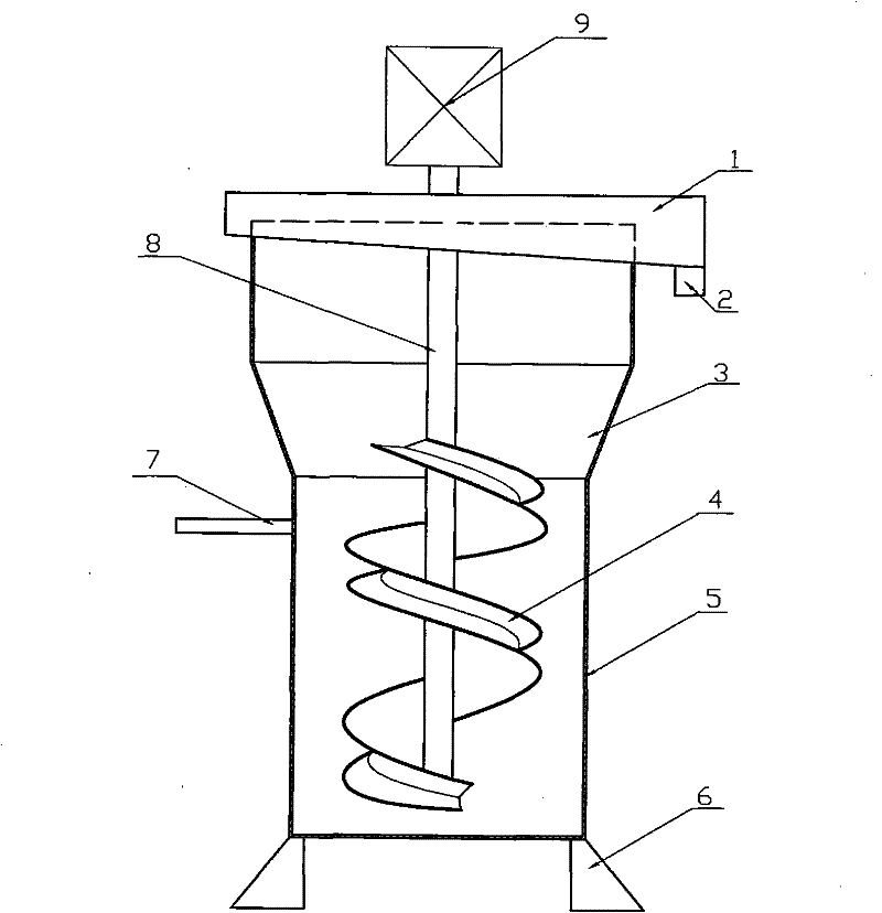
[0034] (2) Wet ball milling and overflow classification are in the wet frequency conversion ball mill classification device (see figure 1 When grinding and grading in ), add media ball and silicon carbide particle sand at the weight ratio of media ball: silicon carbide particle size 4:1. The frequency conversion wet ball mill rotates at 80rpm for 0.5h in the early stage and 100rpm at 2h in the middle. In the later period, the rotation speed is 120 rpm and the water inlet is 600 L / h; the wet variable frequency ball mill classification device includes a vertical cylinder 5 and a double agitating spiral body...

Embodiment 2

[0043] Embodiment 2 A method for preparing a cutting blade material for a semiconductor wafer includes the following steps:

[0044] (1) For raw material crushing, select green silicon carbide blocks with a purity of ≥99% and black silicon carbide blocks with a mass ratio of 19:1, and perform jaw crushing and sieving to collect silicon carbide sand with a particle size of ≤3mm;

[0045] (2) Wet ball milling and overflow classification The same wet frequency conversion ball mill and classification device as in Example 1 is used for wet grinding and classification. When grinding and classifying, the medium ball: silicon carbide particle size sand is 5:1 Add media balls and silicon carbide granular sand to the weight ratio of the medium. The frequency conversion wet ball mill has a rotation speed of 90 rpm in the first 0.6h, 100 rpm in the middle 1.9h, and 150 rpm in the later 1.6h, with a water intake of 500L / h;

[0046] (3) Pickling vacuum dehydration Introduce the above-mentioned sil...

Embodiment 3

[0054] Embodiment 3 is a method for preparing a semiconductor wafer cutting blade material, which is basically the same as embodiment 1, except that: in the step (2), wet grinding is performed by ordinary wet frequency conversion ball mill, and then Commonly used hydraulic classification device performs classification to obtain silicon carbide powder slurry with the required particle size range.

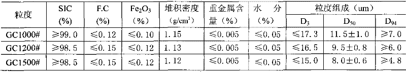
[0055] The performance indexes of the obtained semiconductor wafer cutting blade materials are shown in Table 4.


PUM


Abstract

The invention relates to a preparation method of a semiconductor wafer cutting blade material. In the preparation method, high-purity green silicon carbide and black silicon carbide are adopted as raw materials, and a wafer cutting blade material is prepared through the steps of jaw crushing and sifting, wet ball milling classification, pickling, overflow size separation, concentrating and dewatering, drying, blending, fine screening and the like. Silicon carbide blade materials prepared through the method are most in equiareal shape and keep sharp edges and strong cutting power, can minimizeTTV of a silicon wafer, and have strong adaptability to cutting fluid such as polyethylene glycol and the like because blade material particles have larger specific area and clean surfaces. Products crushed by a wet ball mill are most in equiareal shape, have high output, and can avoid excessive crushing. The preparation method of the invention can reach over 50% of rate of finished products, andproducts milled with the technology have more uniform size and distribution of particles, thereby better cutting effect to silicon wafers can be achieved.

Description

Technical field [0001] The invention relates to the field of multi-line cutting, in particular to a method for preparing a cutting blade material for a semiconductor wafer. Background technique [0002] With the rapid development of the integrated circuit industry, the demand for high-quality semiconductor wafers is increasing day by day. The processing of semiconductor silicon wafers is an important link in integrated circuit manufacturing, and effective silicon wafer cutting technology is the basic guarantee for obtaining high surface accuracy and surface quality silicon wafers. When using traditional diamond inner circle cutting, as the diameter of the wafer continues to increase, the thickness of the blade substrate, the thickness of the cutting edge, and the difficulty of blade tension increase, the loss of notch material and blade wear during cutting increase, and the quality of silicon wafers decreases , It is difficult to cut large diameter wafers. Multi-wire cutting is...

Claims


Application Information

Patent Timeline
Patent Type & Authority Patents(China)
IPC IPC(8): C01B31/36
Inventor 罗小军姜维海宋贺臣郝玉辉李要正
Owner HENAN XINDAXIN SCI & TECH
Why Eureka
Try Eureka