
Production method of silicon wafer cutting blade material

A silicon wafer cutting and production method technology, applied in grain processing, etc., can solve the problems of uneven particle size, poor cutting efficiency, low purity, etc., achieve uniform size distribution, reduce production costs, and reduce emission pollution.

Inactive Publication Date: 2013-09-04
JIANGSU TAYAL PHOTOVOLTAIC AUXILIARY MATERIAL
View PDF4 Cites 2 Cited by
  • Summary
  • Abstract
  • Description
  • Claims
  • Application Information

AI Technical Summary

Problems solved by technology

[0003] At present, the quality of blade materials for photovoltaic wire cutting in China is uneven. Compared with similar foreign products, there are disadvantages such as low purity, uneven particle size, and poor cutting efficiency.
The production equipment and process methods of domestic enterprises are backward, the crushing effect is poor, the particle size distribution of the fine powder is too wide, and the products lack market competitiveness
At present, the production and processing methods of silicon carbide cutting blades in China mainly include the following types: the production process of jet mill crushing, the products produced are more than 90% equal in shape, and the yield is also high, but the overall output of jet mill Low, the shape of the output particles is round, the sharpness is poor, and there are hidden cracks, which is not conducive to cutting; the production process of Raymond mill crushing, although the output is high, but the yield is low, and the output product is relatively small. less, only about 50%, and there are many needle-shaped, flake-shaped and other shaped particles, the cutting efficiency is low and the cutting durability is poor; in the prior art, traditional wet ball mills are also used for crushing, although the product particles are of equal volume It has many shapes and good sharpness, but the output is low, the yield is low, and the over-grinding is serious. In addition, the existing pickling and iron removal process consumes a lot of acid, is poor in economy, and pollutes a lot, which does not meet the trend of environmental protection.

Method used

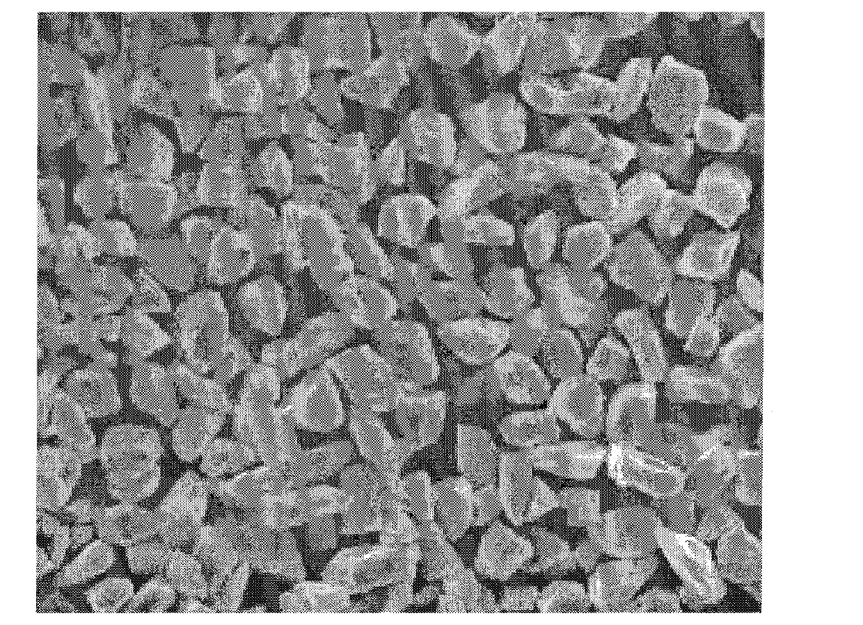
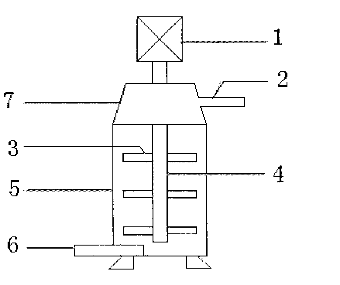
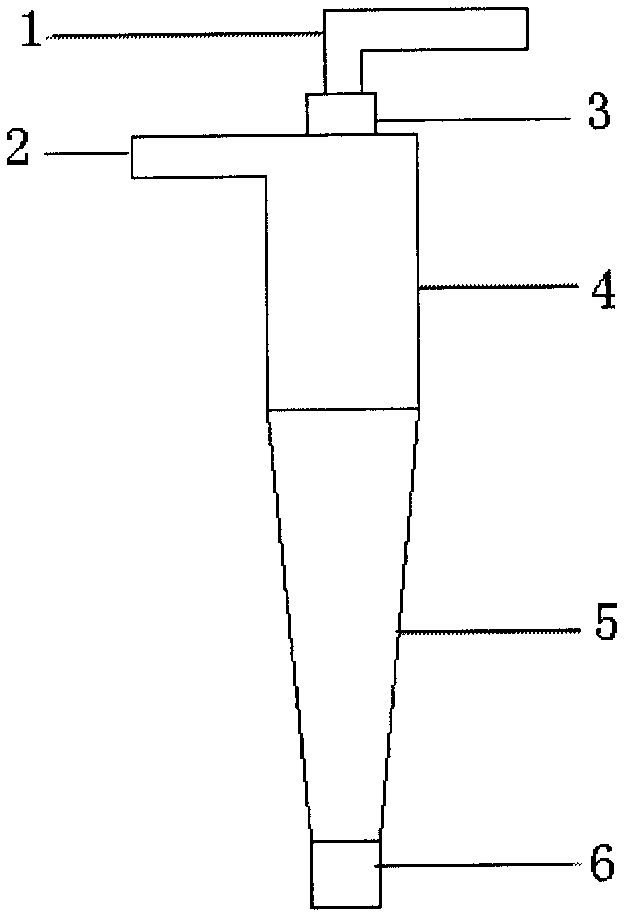

Image

  • Production method of silicon wafer cutting blade material
  • Production method of silicon wafer cutting blade material
  • Production method of silicon wafer cutting blade material

Examples


Embodiment Construction

[0040] A method for preparing a silicon carbide blade for photovoltaic wire cutting, comprising the following steps:

[0041] The first step is to crush the raw materials, select the green silicon carbide block material with a purity ≥ 98% for jaw crushing and sieving, and collect the silicon carbide particle size sand with a particle size ≤ 3mm;

[0042] In the second step of wet ball milling and hydrocyclone classification, the silicon carbide sand particles obtained in the first step are wet ball milled and hydrocyclone classified to obtain a silicon carbide powder slurry in the required particle size range;

[0043] The 3rd step overflows automatic carbon removal, introduces the SiC powder slurry obtained in the second step in the overflow automatic carbon removal equipment, adjusts its mass concentration to 30~50wt%, then adds 30~50ml of flotation oil and 50-70ml of water glass, fully stirred for 0.5-1 hour, then overflowed to remove free carbon;

[0044] The fourth step...


PUM

PropertyMeasurementUnit
particle sizeaaaaaaaaaa

Abstract

The invention relates to a production method of a silicon wafer cutting blade material. The production method of the silicon wafer cutting blade material uses high-purity green silicon carbide as the raw material and comprises the following steps: performing jaw crushing, screening, performing automatic circulation type wet ball milling and hydraulic cyclone classification, performing automatic overflow carbon removal, performing magnetic separation to automatically remove iron, performing alkali washing, cleaning, performing overflow classification under automatic control of a programmable logic controller (PLC), centrifuging to dewater, drying, mixing, performing fine screening and the like. The silicon carbide blade material prepared by the method has equiareal shape, sharp edges and high cutting capability; the blade material particles have large specific surface area and clean appearance and high suitability to cutting fluid such as polyethylene glycol; the product ground by automatic circulation type wet ball milling and cyclone classification has more equiareal shapes, good grain shape and high yield, and overgrinding can be avoided; and automatic magnetic separation is adopted to perform acid-free iron removal, thus the method has high efficiency, environmental friendliness and high degree of automation and is suitable for large-scale production. The product ground by the method has high particle size concentration degree and good grain shape, and better cutting effect can be realized.

Description

technical field [0001] The invention relates to the field of multi-wire cutting, in particular to a method for preparing a blade material silicon carbide for wire cutting of solar photovoltaic silicon wafers. Background technique [0002] With the rapid development of the solar photovoltaic industry, the demand for high-quality silicon wafers is increasing day by day. The processing of silicon wafers is an important link in the manufacture of solar cell groups, and effective silicon wafer cutting technology is the basic guarantee for obtaining high-quality silicon wafers. In recent years, the multi-wire saw (Multi-Wire Saw), which has sprung up suddenly, occupies an absolute market leadership in the field of large-size silicon wafer processing due to its high production efficiency and wafer yield. The mixed cutting agent-mortar used in multi-wire saw, Its role is very important and plays a major role in the cutting process. Silicon carbide micropowder is widely used as a c...

Claims


Application Information

Patent Timeline
Patent Type & Authority Patents(China)
IPC IPC(8): B02C17/16B02C1/02C01B31/36
Inventor 王彭李宏王祎
Owner JIANGSU TAYAL PHOTOVOLTAIC AUXILIARY MATERIAL
Learn More