
Plasma etching method for showing defect of cadmium zinc telluride infrared substrate

A plasma and cadmium zinc telluride technology, which is applied in semiconductor devices, sustainable manufacturing/processing, electrical components, etc., can solve the problems of uncontrollable corrosion depth and fuzzy contour water chestnut, and achieve the effect of enhancing precise controllability

Active Publication Date: 2010-10-27
SHANGHAI INST OF TECHNICAL PHYSICS - CHINESE ACAD OF SCI
View PDF3 Cites 10 Cited by
  • Summary
  • Abstract
  • Description
  • Claims
  • Application Information

AI Technical Summary

Problems solved by technology

However, the defect visualization method of wet chemical corrosion has the disadvantages of uncontrollable corrosion depth and blurred outline

Method used


Image

  • Plasma etching method for showing defect of cadmium zinc telluride infrared substrate
  • Plasma etching method for showing defect of cadmium zinc telluride infrared substrate
  • Plasma etching method for showing defect of cadmium zinc telluride infrared substrate

Examples


Embodiment Construction

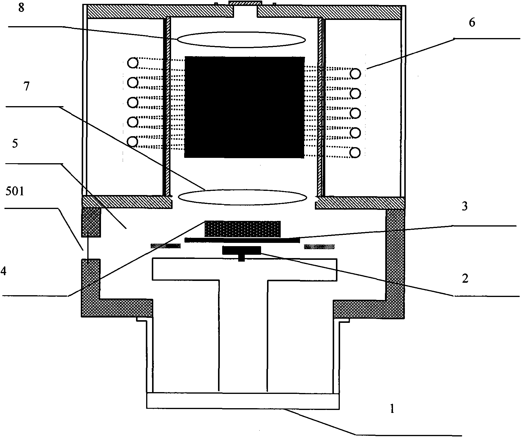
[0017] See figure 1 , the present invention uses British OXFORD company model to be the ICP enhanced RIE equipment of ICP65-80Plus. The equipment includes: a cavity 5 with a vacuum system 1, an RF source 2 for controlling plasma etching energy is placed in the cavity from bottom to top, a sample stage 3 with a temperature control system, and a lower intake coil 7 to generate plasma Body concentration RF source 6, upper intake coil 8. During etching, the etching sample 4 is fixed on the temperature-controlled sample stage 3 , and the etching situation of the sample can be observed in real time through the observation window 501 .

[0018] We take Cd 1-x Zn x Te (x=0.04) epitaxial material is a sample, and the method of the present invention is described in further detail:

[0019] A. Sample cleaning: The CZT substrate sample 4 was cleaned in three organic solvents of trichlorethylene, acetone and alcohol at 65° C. respectively.

[0020] B. Use vacuum grease to paste the CZ...


PUM

PropertyMeasurementUnit
Etching poweraaaaaaaaaa

Abstract

The invention discloses a plasma etching method for showing defect of a cadmium zinc telluride (CZT) infrared substrate, and relates to the material testing technology of the photoelectric probe. The plasma etching method adopts the technical scheme that the defect of the infrared CZT substrate is shown by enhancing the reactive ion etching (RIE) with high-density low-energy inductively coupled plasma (ICP), so the method skillfully utilizes the accuracy controllability of the etching rate of the ICP-enhanced RIE and the inconsistency at a normal region and a defective region of the infrared CZT substrate and thus effectively solves the problems of uncontrollable substrate removal rate and blurred outline of the defect existing in a conventional defect showing method. The method has the characteristics of simple process, high stability and clear showing.

Description

technical field [0001] The invention relates to a detection technology of a photoelectric detection device material, in particular to a defect display method of an infrared substrate material of a photosensitive element chip of an infrared focal plane array device. Background technique [0002] Infrared focal plane array device is an advanced imaging sensor with both infrared information acquisition and information processing functions. There are important and extensive applications in military and civilian fields. Due to its irreplaceable status and role, major industrial countries in the world have listed the preparation technology of infrared focal plane array devices as a high-tech project for key development. [0003] Driven by the advanced infrared application system, infrared detection technology has entered an important development stage of the third generation infrared focal plane detector characterized by large area array, miniaturization and multicolor, see S.Hor...

Claims


Application Information

Patent Timeline
IPC IPC(8): H01L31/18
CPCY02P70/50
Inventor 叶振华尹文婷王建新方维政杨建荣陈昱林春胡晓宁丁瑞军何力
Owner SHANGHAI INST OF TECHNICAL PHYSICS - CHINESE ACAD OF SCI
Learn More