Check patentability & draft patents in minutes with Patsnap Eureka AI!

Silicon slice-In2O3 flower-like nano structure compounded semiconductor material and preparation method thereof

A nanostructure and semiconductor technology, applied in the field of semiconductor materials and devices, and optoelectronic materials, can solve the problems of high cost and harsh preparation method conditions, and achieve the effect of low cost, simple method and lower requirements

Inactive Publication Date: 2010-11-03
EAST CHINA NORMAL UNIVERSITY
View PDF0 Cites 0 Cited by
  • Summary
  • Abstract
  • Description
  • Claims
  • Application Information

AI Technical Summary

Problems solved by technology

[0005] The second object of the present invention is to provide compound In on silicon chip 2 o 3 Preparation method of flower-like nanostructure semiconductor materials to solve the existing In 2 o 3 The problem of harsh conditions and high cost in the preparation of nanomaterials provides a new method with low cost and high repeatability

Method used


Image

  • Silicon slice-In2O3 flower-like nano structure compounded semiconductor material and preparation method thereof
  • Silicon slice-In2O3 flower-like nano structure compounded semiconductor material and preparation method thereof
  • Silicon slice-In2O3 flower-like nano structure compounded semiconductor material and preparation method thereof

Examples


Embodiment 1

[0020] a. Clean the silicon wafer and cut it into 1.5cm×1.5cm pieces;

[0021] b. Heating the horizontal tubular growth furnace to 900°C at a rate of 5°C / min;

[0022] c. Mix 0.2g Sn powder, 2g In 2 o 3 Powder and 6g of C powder are mixed as a source and placed in a quartz boat, and a small piece of clean silicon wafer is covered on the quartz boat as a substrate to collect the reaction product. The vertical distance between the silicon wafer and the source is 4mm;

[0023] d. Put the quartz boat in the middle of the preheated horizontal tube furnace;

[0024] e. The inert gas Ar with a flow rate of 0.5L / min was introduced as a carrier gas, and the reaction was carried out at atmospheric pressure for 240 minutes;

[0025] f. Take out the quartz boat and the silicon chip, and a layer of light yellow substance grows on the silicon chip, which means the required material is obtained.

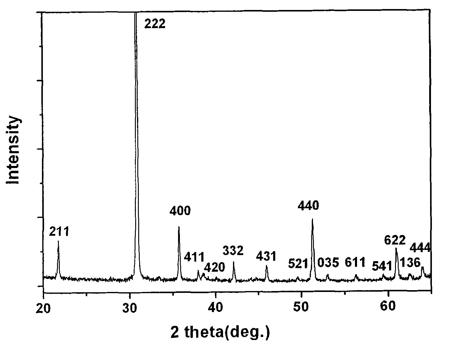
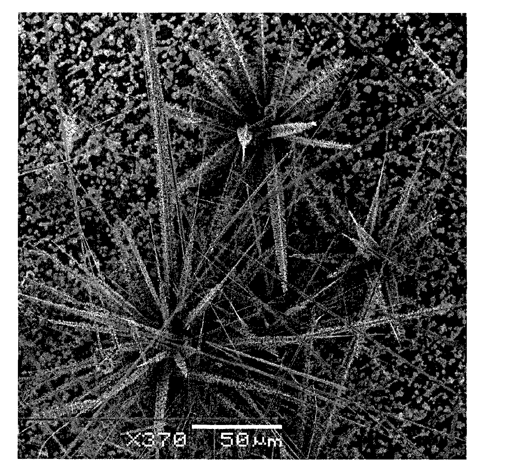
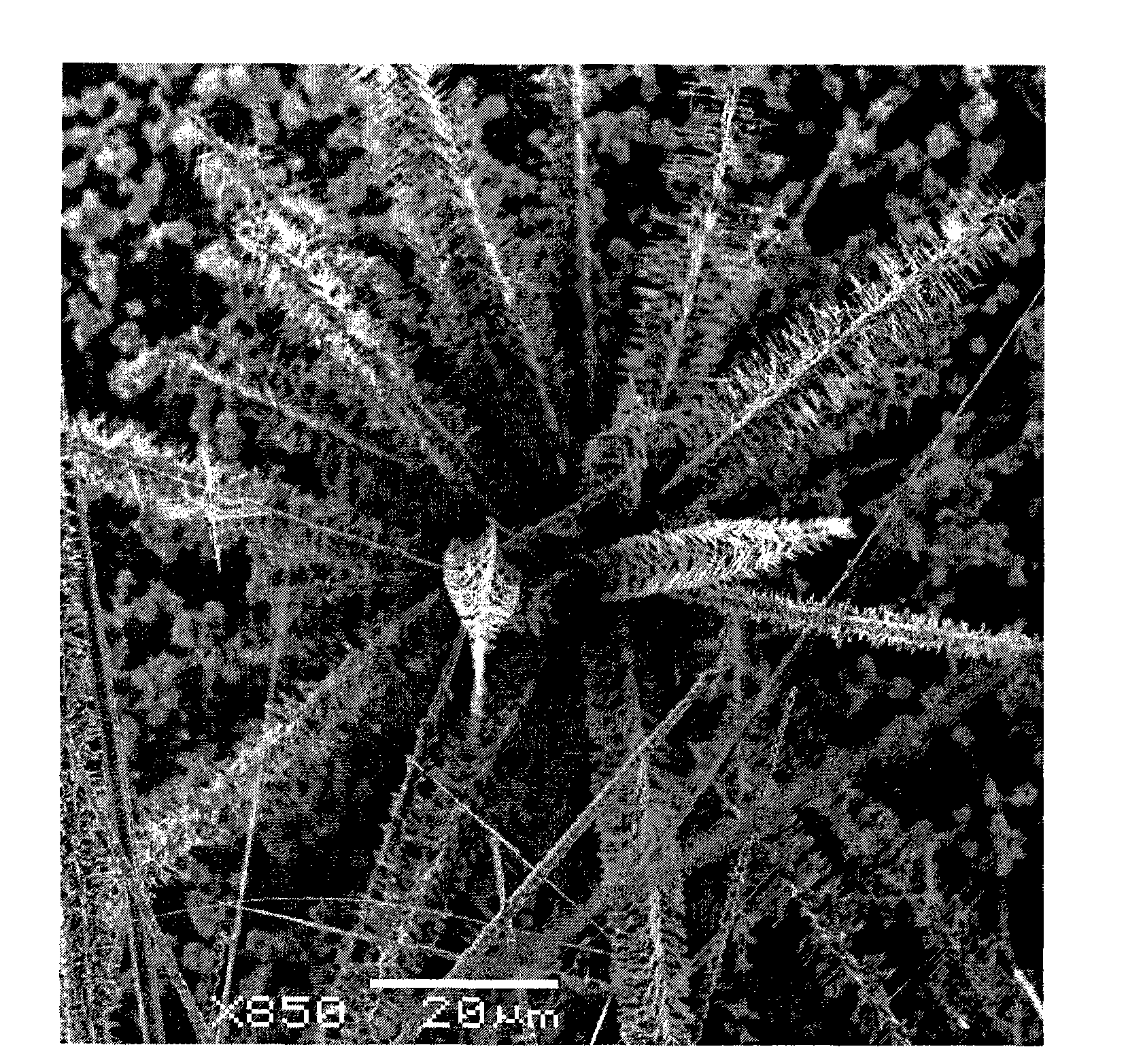
[0026] Detect the prepared material, and the test results are as follows: figure 1 , 2 , ...

Embodiment 2

[0028] a. Clean the silicon wafer and cut it into 1.8cm×1.8cm pieces;

[0029] b. Heating the horizontal tubular growth furnace to 850°C at a rate of 5°C / min;

[0030] c. Mix 0.1g Sn powder, 1g In 2 o 3 Powder and 3g of C powder are mixed as a source into a quartz boat, and a small piece of clean silicon wafer is covered on the quartz boat as a substrate to collect the reaction product. The vertical distance between the silicon wafer and the source is 5mm;

[0031] d. Put the quartz boat in the middle of the preheated horizontal tube furnace;

[0032] e. The inert gas Ar with a flow rate of 0.3L / min was introduced as a carrier gas, and the reaction was carried out at atmospheric pressure for 200 minutes;

[0033] f. Take out the quartz boat and the silicon chip, and a layer of light yellow substance grows on the silicon chip, which means the required material is obtained.


PUM

PropertyMeasurementUnit
Lengthaaaaaaaaaa
Lengthaaaaaaaaaa

Abstract

The invention discloses a silicon slice-In2O3 flower-like nano structure compounded semiconductor material and a preparation method thereof. The material comprises a substrate, wherein the substrate is a silicon slice, and In2O3 crystals are grown on the surface of the substrate; and the In2O3 crystals have a flower-like nano structure which is formed by connecting the bottom parts of burred rod-like nano structures, the length of the In2O3 burred rod-like nano structures is 40 to 80 micrometers, the length of the burred nano structures is 0.8 to 4.6 micrometers, and the burred nano structures are arranged on the surfaces of the rod-like nano structures orderly. In the preparation method, Sn powder, In2O3 powder and C powder are used as a raw material, and the In2O3 flower-like nano structures are grown by a thermal evaporation method. The surfaces of the flower-like structures of the invention have a large amount of nano tips which can be used as emitting points, and therefore can serve as good field emitting cathode material. The material has the advantages of low cost, high repeatability, and the like. By combining with the conventional mature semiconductor silicon integrated circuit process, the material is suitable to be used for preparing integrated nano optoelectronic devices.

Description

technical field [0001] The invention relates to the technical field of optoelectronic materials, semiconductor materials and devices, in particular to a method for compounding In on a silicon wafer. 2 o 3 Semiconductor material with flower-like nanostructure and method for its preparation. Background technique [0002] In 2 o 3 It is a wide-bandgap transparent semiconductor material with a direct bandgap in the range of 3.55-3.75eV, good electrical conductivity and high light transmittance. Due to its unique electrical, chemical and optical properties, In 2 o 3 It has a wide range of applications in the fields of chemistry, biosensing, solar cells, photocatalysis, actuators, optoelectronics, and flat panel displays. [0003] Recently, various methods (solution method, molecular beam epitaxy, pulsed laser deposition, metal-organic chemical vapor deposition, etc.) have been used to prepare various In 2 o 3 Nanostructures, such as nanowires, nanobelts, nanocubes, octahe...

Claims


Application Information

Patent Timeline
IPC IPC(8): C04B41/50
Inventor 黄雁君郁可朱自强
Owner EAST CHINA NORMAL UNIVERSITY
Features
  • R&D
  • Intellectual Property
  • Life Sciences
  • Materials
  • Tech Scout
  • Unparalleled Data Quality
  • Higher Quality Content
  • 60% Fewer Hallucinations
Learn More