IGBT with improved collector structure

A collector and collector area technology, applied in the direction of circuits, electrical components, semiconductor devices, etc., can solve the problems of reducing the impact resistance of devices, increasing on-state loss, increasing reverse recovery hardness, etc., to achieve turn-off loss and endurance Good impact performance, reduced overshoot voltage, and improved impact resistance

Active Publication Date: 2013-01-02
WUXI NCE POWER
View PDF1 Cites 0 Cited by
  • Summary
  • Abstract
  • Description
  • Claims
  • Application Information

AI Technical Summary

Problems solved by technology

The denser the doping concentration of the P-type collector region, the higher the injection efficiency of the P-type collector region as the emitter region of the PNP bipolar transistor when the IGBT is in the forward conduction state, and the greater the hole current will be. , so that the on-state voltage drop will be lower; however, due to the increase in injection efficiency, the reverse recovery charge, reverse recovery time and tail current of the device will all increase, increasing the power loss when the device is turned off, and , due to the very large concentration gradient between the P-type collector region and the N-type drift region, the number of minority carriers injected into the P-type collector region is very limited, and these minority carriers are quickly swept away during the reverse recovery process. Out or compound, increase the hardness of reverse recovery, that is, the S value is small, reducing the impact resistance of the device
On the contrary, if the impurity concentration of the P-type collector area is reduced, the on-state voltage drop of the device will increase, resulting in an increase in on-state loss, which is also not conducive to device performance.

Method used


Image

  • IGBT with improved collector structure
  • IGBT with improved collector structure
  • IGBT with improved collector structure

Examples


Embodiment 1

[0023] like Figure 4As shown: on the section of the insulated gate bipolar transistor IGBT, the N-type semiconductor substrate includes an N-type drift region 7, and the N-type drift region 7 has two opposite main surfaces, and the two opposite main surfaces include the first A main surface 15 and a second main surface 16 . A P-type collector region 8 is formed on the second main surface 16 of the N-type drift region 7, and the P-type collector region 8 includes one or more first regions 11 and one or more second regions 14 , the first region 11 and the second region 14 are both of P conductivity type; the first region 11 surrounds a plurality of second regions 14 or the second regions 14 are alternately adjacent to the first regions 11 . In this embodiment, the second regions 14 are alternately adjacent to the first regions 11 . The first region 11 has a first doping concentration, the second region 14 has a second doping concentration, the first doping concentration of th...

Embodiment 2

[0027] like Figure 5 Shown: It is an insulated gate bipolar transistor IGBT with a trench-type insulated gate structure. On the cross section of the insulated gate bipolar transistor IGBT, a P base region 1 is arranged on the upper part of the N-type drift region 7 , and the P base region 1 penetrates the N-type drift region 7 . A trench 12 is provided in the P base region 1 , and the trench 12 is located in the P base region 1 and extends deep to the N-type drift region 7 below the P base region 1 . An insulating oxide layer 3 grows on the inner wall of the trench 12 , and conductive polysilicon 4 is deposited in the trench 12 on which the insulating oxide layer 3 grows. An N-type emitter region 2 is arranged above the outer wall of the trench 12 , and the N-type emitter region 2 is in contact with the outer wall of the trench 12 . The notch of the trench 12 is covered by an insulating dielectric layer 10 , and a metallized emitter 6 is also deposited on the first main sur...

Embodiment 3

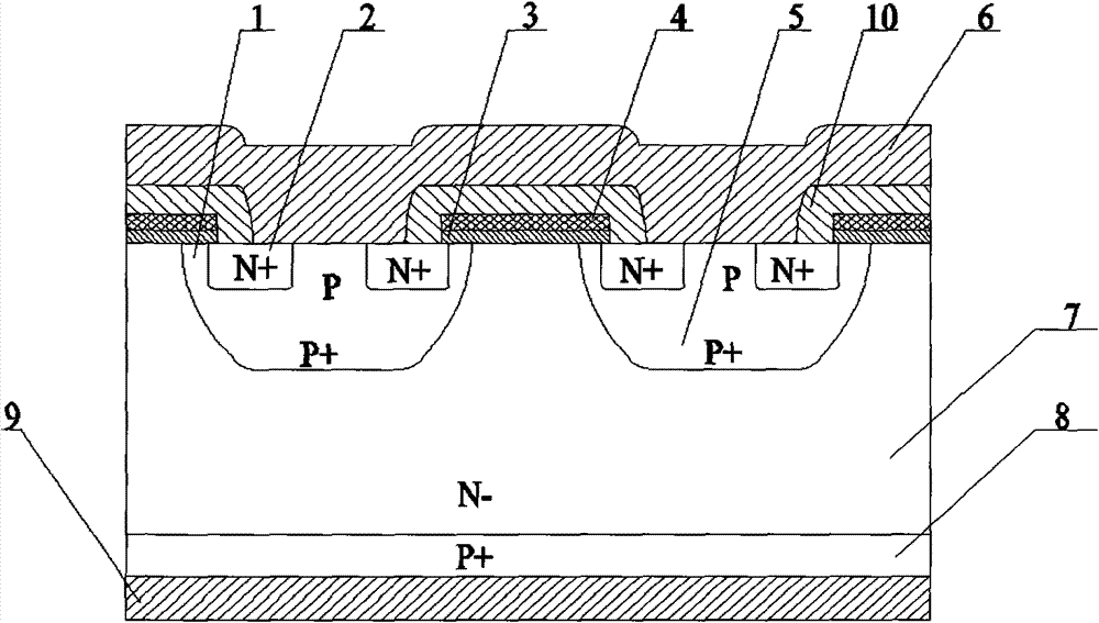
[0030] like Image 6 As shown: it is an insulated gate bipolar transistor IGBT adopting a planar insulated gate structure, and an N+ collector short-circuit region 13 is provided in the P-type collector region 8 . like Image 6 As shown: the upper part of the N-type drift region 7 is provided with a P base region 1, and the P base region 1 is provided with two N-type emitter regions 2; the adjacent P base region 1 uses an N-type drift region 7 phase isolation. The bottom of the P base region 1 is provided with a P+ base region 5 . The first main surface 15 of the N-type drift region 7 is provided with a planar insulating gate structure; the insulating gate includes an insulating oxide layer 3 and a conductive polysilicon 4; the insulating oxide layer 3 is in phase with the N-type drift region 7 The adjacent P base region 1 is in contact with the corresponding N-type emitter region 2 in the P base region 1 . The insulating oxide layer 3 and the conductive polysilicon 4 are ...


PUM


Abstract

The invention relates to an insulated gate bipolar translator (IGBT) with an improved collector structure. The IGBT comprises a semiconductor substrate, wherein the second main surface of the semiconductor substrate is provided with a second conductive type collecting region and a metalized collector; a second conductive type base region is arranged in the semiconductor substrate; the upper part of the second conductive type base region is provided with a first conductive type emitting region; the first main surface of the semiconductor is provided with an insulated gate, an insulated dielectric layer and a metalized emitter; the second conductive type collecting region comprises one or more first regions with a first doping density and one or more second regions with a second doping density; the first regions surround the plurality of the second regions or the first regions and the second regions are arranged alternately and adjacently; the first doping density of the first regions is less than the second doping density of the second regions; and the first doping density of the first regions is greater than the doping density of the first conductive type conductive substrate. TheIGBT has the characteristics of low on-state voltage, lower turn-off loss and higher impact resistance performance.

Description

technical field [0001] The invention relates to a power semiconductor device, in particular to an IGBT with an improved collector structure. Background technique [0002] The insulated gate bipolar transistor IGBT (Insulated Gate Bipolar Transistor) was proposed and rapidly promoted in the 1980s, and has been widely used in the field of medium and high voltage and high current. ) pushes power electronics technology to the high frequency era, compared with other kinds of power semiconductors, such as bipolar transistors and MOSFETs; the insulated gate bipolar transistors can handle higher power with lower power loss, and can Working in high-frequency circuits is the most prominent feature and advantage of IGBT. At present, the types of IGBTs that have been widely produced and used include: punch-through IGBT (PT-IGBT), non-punch-through IGBT (NPT-IGBT), and field-stop IGBT (FS-IGBT). The original intention and goal of reducing power loss and increasing operating frequency w...

Claims


Application Information

Patent Timeline
Patent Type & Authority Patents(China)
IPC IPC(8): H01L29/739H01L29/36
Inventor 朱袁正叶鹏胡永刚
Owner WUXI NCE POWER
Why Eureka
Try Eureka