Surface cleaning method of polished silicon substrate material

A technology of silicon substrate and back surface is applied in the field of surface cleaning after silicon substrate material polishing, which can solve the problems of high surface tension of polishing liquid, heavy metal pollution of silicon substrate, and high surface energy, so as to avoid particle scratches and achieve a perfect surface. Quality, the effect of improving perfection

Inactive Publication Date: 2010-12-08
HEBEI UNIV OF TECH
View PDF5 Cites 5 Cited by
  • Summary
  • Abstract
  • Description
  • Claims
  • Application Information

AI Technical Summary

Problems solved by technology

[0004] The present invention aims to overcome the deficiencies in the prior art and provide a simple, easy, pollution-free and clean method for cleaning the surface of the silicon substrate material after polishing, which solves the problem of high energy on the surface of the silicon substrate wafer after the silicon substrate material is polished. Adsorption of abrasive particles causes surface scratches, residual polishing fluid has a high surface tension and is easy to spheroidize, and continues to chemically react with the surface of the silicon substrate, resulting in uneven corrosion of the silicon substrate, and the conversion of contaminated heavy metal ions into atoms and formation of silicon atoms on the surface of the silicon substrate Alloys cause heavy metal contamination of silicon substrates

Method used


Image

  • Surface cleaning method of polished silicon substrate material
  • Surface cleaning method of polished silicon substrate material
  • Surface cleaning method of polished silicon substrate material

Examples


Embodiment 1

[0021] (1) Preparation of cleaning solution: parts by weight (parts)

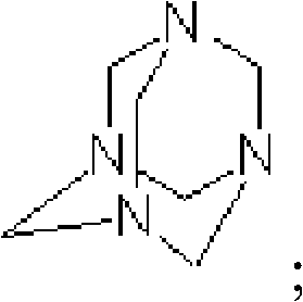
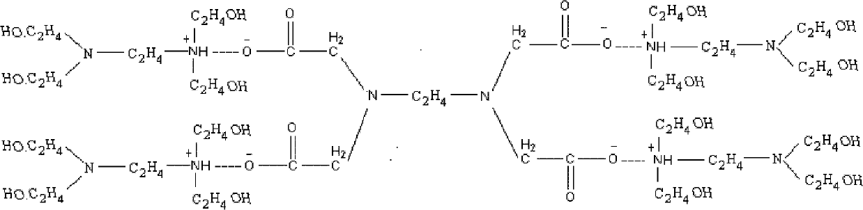
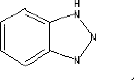
[0022] Add 50g of FA / O surfactant, 75g of FA / OII type chelating agent, and 75g of FA / OII type composite corrosion inhibitor into 2300g of ultra-pure deionized water above 18MΩ, stir evenly while adding, and prepare 2500g of cleaning solution ;Use the prepared cleaning solution to polish and clean the silicon substrate material after alkaline chemical mechanical polishing at a low pressure below 3000Pa and a large flow rate of 4000ml / min, and the polishing and cleaning time is 2min, so that the surface of the silicon substrate material clean. The silicon substrate surface after cleaning has no corrosion patterns, and the surface roughness is Ra=0.3nm (10 μm×10 μm).

Embodiment 2

[0024] (1) Preparation of cleaning solution: parts by weight (parts)

[0025] Add 50g of FA / O surfactant, 10g of FA / OII type chelating agent, and 20g of FA / OII type composite corrosion inhibitor into 2200g of ultra-pure deionized water above 18MΩ, stir evenly while adding, and prepare 3000g of cleaning solution ;Use the prepared cleaning solution to polish and clean the silicon substrate material after alkaline chemical mechanical polishing at a low pressure below 1000Pa and a large flow rate of 5000ml / min, and the polishing and cleaning time is 1min, so that the surface of the silicon substrate material clean. The silicon substrate surface after cleaning has no corrosion patterns, and the surface roughness is Ra=0.2nm (10 μm×10 μm).

[0026] The role of the technology used is: after the silicon substrate material is alkaline polished, there are problems such as high energy, high surface tension, uneven distribution of residual polishing liquid, and contamination of metal ion...


PUM


Abstract

The invention relates to a surface cleaning method of a polished silicon substrate material, which is characterized by comprising the following concrete steps of: taking 0.5-5 parts of nonionic surfactant, 0.1-5 parts of FA/OII type chelating agent, 0.1-5 parts of FA/O II type compound corrosion inhibitor and the balance of deionized water in parts by weight, and uniformly stirring to prepare a water-soluble surface cleaning solution with the pH value of 6.5-7.6; carrying out polishing cleaning on a silicon substrate material subjected to alkaline chemical-mechanical polishing by using the cleaning solution obtained in the step 1 under the conditions of less than 4000Pa of low pressure and 400-5000ml/minute of large flow, wherein the polishing cleaning time is at least 30 seconds-3 minutes, so that the surface of the silicon substrate material is clean. The invention has the advantages that low-pressure large-flow cleaning is carried out on the silicon substrate material by immediately using the cleaning solution after the polishing process in a CMP (Chemical-Mechanical Polishing) working procedure, and a clean and perfect polished surface can be obtained.

Description

technical field [0001] The invention belongs to the cleaning technology of semiconductor materials, in particular to a method for cleaning the surface of a silicon substrate material after CMP after polishing. Background technique [0002] Crystalline silicon is gray-black, belongs to atomic crystal, is hard and has metallic luster, and has semiconductor properties. The chemical properties of silicon are relatively active. It can combine with oxygen and other elements at high temperature. It is insoluble in water, nitric acid and hydrochloric acid, but soluble in hydrofluoric acid and lye. Monocrystalline silicon is an important semiconductor material used in the manufacture of high-power transistors, rectifiers, solar cells, and more. [0003] Silicon substrate is currently the most common substrate material. As a substrate material, the crystal surface is required to be ultra-smooth and ultra-clean. Studies have shown that the quality of the device depends largely on the...

Claims


Application Information

Patent Timeline
Patent Type & Authority Applications(China)
IPC IPC(8): C23G5/036
Inventor 刘玉岭孙鸣杨金波何彦刚
Owner HEBEI UNIV OF TECH
Why Eureka
Try Eureka