Micro semiconductor laser diode capable of realizing high power single-mode output and manufacturing method thereof
A laser diode and semiconductor technology, applied to the structure of the active region, the structure of the optical resonant cavity, etc., can solve the problems of increasing the length of the diode, reducing the cost of laser diode production, etc. Die output, the effect of increasing the number of qualified chip products
- Summary
- Abstract
- Description
- Claims
- Application Information
AI Technical Summary
Problems solved by technology
Method used
Image
Examples
Embodiment approach 1
[0049] Figure 4-6 The non-rectangular resonator semiconductor laser diode of the first embodiment of the present invention will be described. see Figure 4 In the top view of the chip surface, the two ends of the resonant cavity and the parts close to the vertical end face have a rectangular structure, and the middle part of the resonant cavity has a non-rectangular structure.
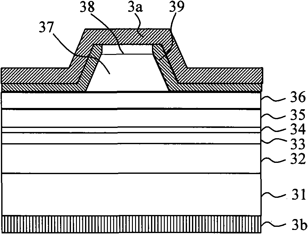
[0050] Figure 5 for along Figure 4 The cross-section of the dotted line A-A in the figure shows a single-channel waveguide structure. According to the wavelength selection, the width of the waveguide channel can only support single-mode transmission, such as an infrared laser with a wavelength of 800nm, and the width of the ridge bottom 571 can be 2.5-4 μm. refer to Figure 5 , including an n-type AlGaAs buffer layer 52, an n-type AlGaAs cladding layer 53, an AlGaAs light-emitting layer 54, a first p-type AlGaAs cladding layer 55, and a p-type InGaP etch stop layer 56 from the n-type GaAs substr...
Embodiment approach 2
[0060] In the second embodiment of the present invention, the two ends of the resonant cavity of the semiconductor laser diode chip and the adjacent part of the vertical end face are rectangular single-channel waveguide structures, and the middle part of the resonant cavity is as follows: Figure 14 A non-rectangular single-channel waveguide structure is shown, but with a larger width chosen to increase the cross-sectional area and thus increase the peak optical output power. The manufacturing method of the non-rectangular resonator semiconductor laser diode of the second embodiment of the present invention is similar to the manufacturing method of the non-rectangular resonator semiconductor laser diode of the first embodiment, and the difference is to select such as Figure 15 The mask pattern shown is used for photolithography and subsequent etching processes.
Embodiment approach 3
[0062] In the third embodiment of the present invention, the two ends of the resonant cavity of the semiconductor laser diode chip and the adjacent part of the vertical end face are rectangular single-channel waveguide structures, and the middle part of the resonant cavity is as follows: Figure 16 In the shown non-rectangular three-channel waveguide structure, each waveguide channel generates photons after introducing current, oscillates and amplifies in its own waveguide, and merges in the common single-channel waveguide part to increase the optical output power. The manufacturing method of the non-rectangular resonator semiconductor laser diode of the third embodiment of the present invention is similar to the manufacturing method of the non-rectangular resonator semiconductor laser diode of the first embodiment, and the difference is to select such as Figure 17 The mask pattern shown is used for photolithography and subsequent etching processes.
PUM
 Abstract
Description
Claims
Application Information
 - R&D
- Intellectual Property
- Life Sciences
- Materials
- Tech Scout
- Unparalleled Data Quality
- Higher Quality Content
- 60% Fewer Hallucinations
Browse by: Latest US Patents, China's latest patents, Technical Efficacy Thesaurus, Application Domain, Technology Topic, Popular Technical Reports.
© 2025 PatSnap. All rights reserved.Legal|Privacy policy|Modern Slavery Act Transparency Statement|Sitemap|About US| Contact US: help@patsnap.com


