
A/D converter, solid-state image capturing apparatus and electronic information device

一种转换器、端子的技术,应用在A/D转换器、固态图像捕捉装置和电子信息设备领域,能够解决未被充分稳定等问题

Active Publication Date: 2010-12-22
SHARP KK
View PDF3 Cites 12 Cited by
  • Summary
  • Abstract
  • Description
  • Claims
  • Application Information

AI Technical Summary

Problems solved by technology

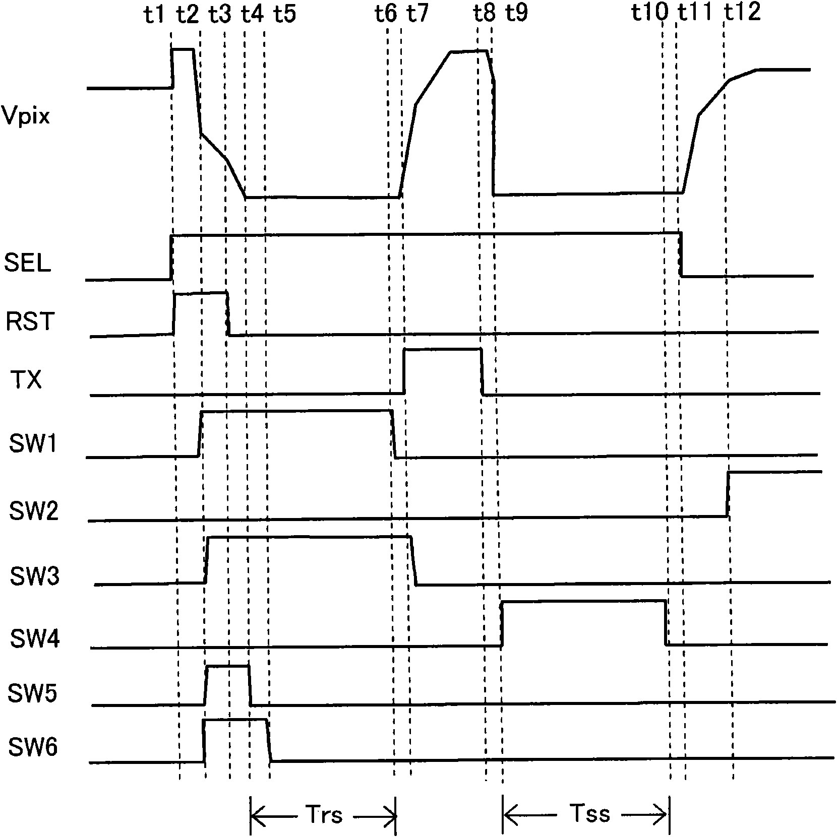
[0036] Instead, as in Figure 13 As shown in the timing chart of , in the case where both the reset sampling period Trs and the signal sampling period Tss are extremely short for the pixel signal Vpix in the A / D converter of the conventional art, when the pixel signal Vpix is ​​not sufficiently stabilized Simultaneously the sampling of the pixel signal Vpix is ​​performed in the sample and hold circuit 4A1

Method used


Image

  • A/D converter, solid-state image capturing apparatus and electronic information device
  • A/D converter, solid-state image capturing apparatus and electronic information device
  • A/D converter, solid-state image capturing apparatus and electronic information device

Examples


Embodiment 1

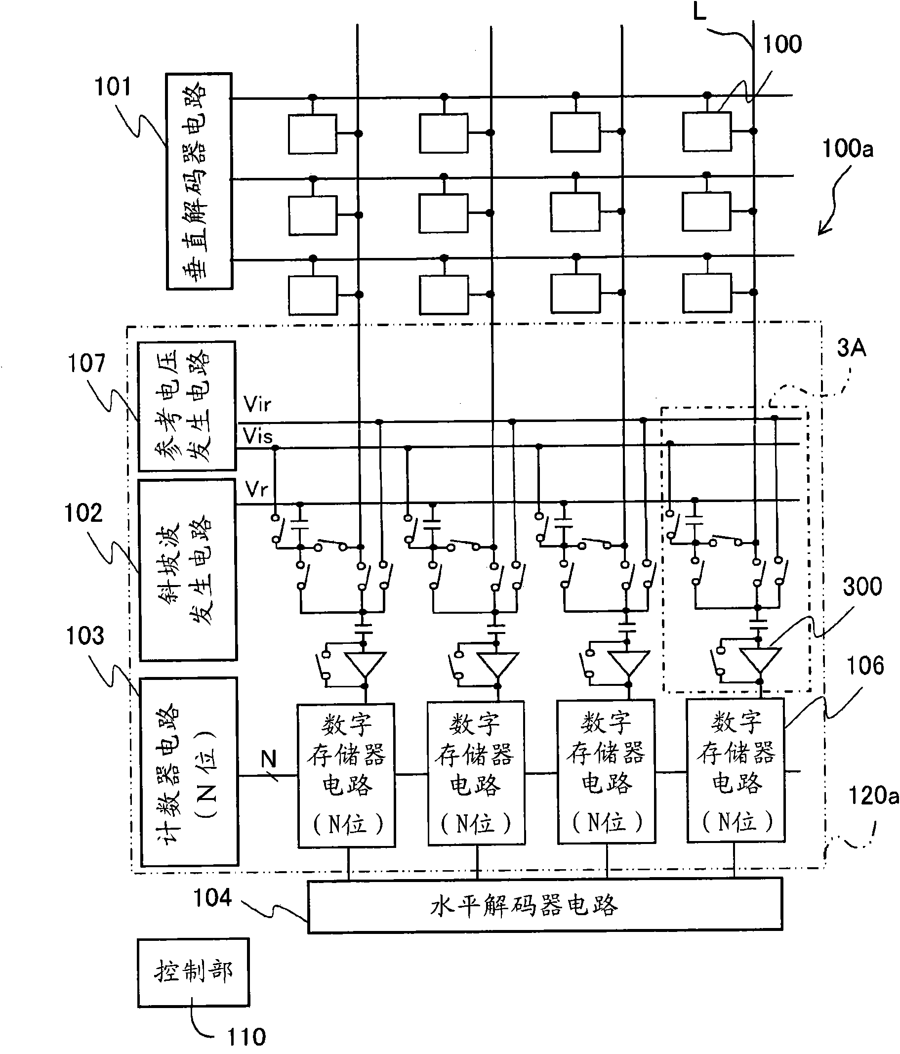
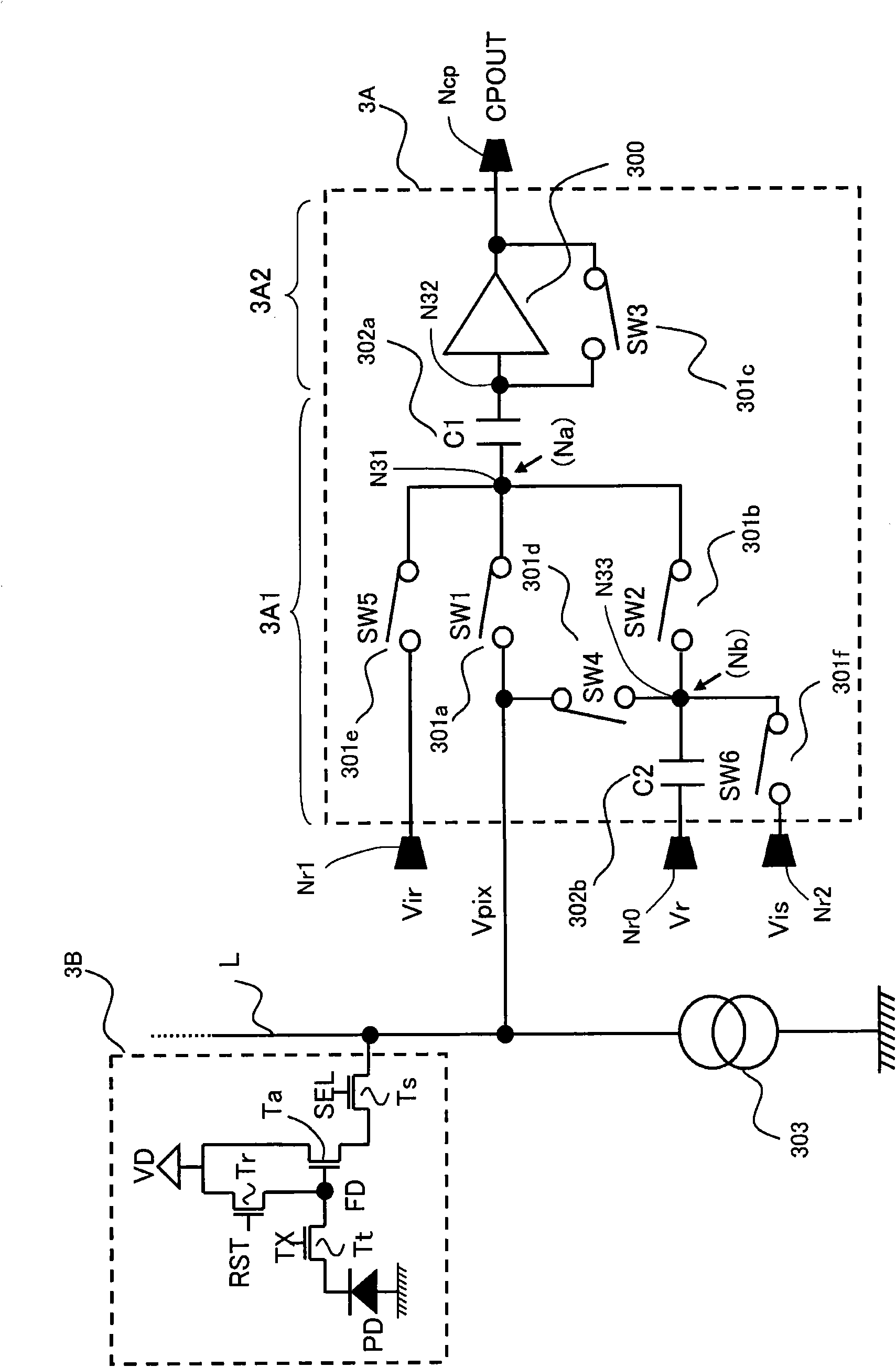
[0107] figure 1 is a diagram describing a system configuration of a CMOS image sensor including an A / D converter according to Embodiment 1 of the present invention. figure 2 is a diagram showing the configuration of a sample hold circuit and a comparison circuit section and pixels in the A / D converter according to Embodiment 1 of the present invention.

[0108] Note that in Embodiment 1 and other embodiments described below, switches, comparison circuits, and digital memory circuits will become the models shown in the drawings unless otherwise specified. Furthermore, it goes without saying that the embodiments of the present invention will be limited to the exemplary configuration of the CMOS image sensor explained hereinafter.

[0109] The CMOS image sensor 100a according to Embodiment 1 includes: a plurality of pixels 100 arranged in rows and columns; a vertical decoder circuit 101 for selecting a pixel row of the plurality of pixels 100 arranged in rows and columns; and ...

Embodiment 2

[0171] Figure 7 is a diagram describing a solid-state image capture device according to Embodiment 2 of the present invention, showing specific elements constituting a sample-hold circuit and a comparison circuit section of an A / D converter in the solid-state image capture device. Figure 8 is a diagram describing an A / D converter in a solid-state image capturing device according to Embodiment 2 of the present invention, showing a sample hold circuit and a comparison circuit section in the A / D converter, and a configuration of pixels.

[0172] In the A / D converter according to Embodiment 2, and further in the sample hold circuit and comparison circuit section (SHC circuit section) 12A therein, the sample hold circuit 12A1 includes: two capacitive elements 1202a and 1202b (hereinafter , each of which is referred to as C1 and C2); and five switches 1201a, 1201b, 1201d, 1201e, and 1201f (hereinafter, each switch is referred to as SW1, SW2, SW4, SW5, and SW6). In addition, the c...

Embodiment 3

[0207] Figure 10 is a block diagram schematically showing an exemplary configuration of an electronic information apparatus as Embodiment 3 of the present invention including the solid-state image capturing device according to Embodiment 1 or 2 used in its image capturing section.

[0208] like Figure 10 The illustrated electronic information apparatus 90 according to Embodiment 3 of the present invention includes any one of the solid-state image capturing devices according to Embodiments 1 and 2 of the present invention as an image capturing section 91 for capturing a subject. The electronic information device 90 also includes at least any one of the following items: a memory section 92 (such as a recording medium) for recording an image after performing predetermined signal processing on high-quality image data captured by the image capturing section for recording Data is subjected to data recording; a display section 93 (such as a liquid crystal display device) for displ...


PUM


Abstract

The invention relates to an A / D converter, solid-state image capturing apparatus and electronic information device. The CMOS image sensor according to the present invention includes a sample hold section 3A1 for retaining an analog input signal voltage and a ramp wave signal voltage; and a comparing section 3A2 for taking an output from the sample hold section 3A1 as an input to compare it with areverse level of itself, in which the sample hold section 3A1 applies a stabilization promoting voltage to a terminal of the sampling capacitance element so that an electric potential level of the terminal of the sampling capacitance element is promoted to become stabilized at a predetermined voltage, when the analog input signal is applied to the terminal of the sampling capacitance element.

Description

[0001] Pursuant to Title 35, United States Code, Section 119(e), this nonprovisional application claims priority to Patent Application No. 2009-142491 filed in Japan on June 15, 2009, the entire contents of which are incorporated herein by reference. technical field [0002] The present invention relates to A / D converters, solid-state image capture devices, and electronic information equipment, and more particularly, to A / D converters for converting analog signals into digital data, solid-state An image capture device, and electronic information equipment including the solid-state image capture device used therein. The present invention is based on the underlying technology of column-parallel A / D converters, wherein a sample-hold section and a comparison section are arranged for each column, and it is used in CCD and CMOS image sensors, near-infrared and far-infrared image sensors, etc., wherein , an element for converting energy into electrons (including a photoelectric conve...

Claims


Application Information

Patent Timeline
Patent Type & Authority Applications(China)
IPC IPC(8): H03M1/12H04N5/335H01L27/146H03M1/56H04N5/357H04N5/363H04N5/369H04N5/374H04N5/3745H04N5/378
CPCH04N5/378H03M1/56H03M1/1295H03M1/0607H03M1/123H04N5/37457H04N25/778H04N25/75
Inventor 星野幸三
Owner SHARP KK
Learn More