Method for extracting polysilicon through electron beams and acid washing

A technology of polysilicon and electron beams, which is applied in chemical instruments and methods, silicon compounds, sustainable manufacturing/processing, etc., can solve the problems that affect the photoelectric conversion efficiency of solar cells, consume a lot of energy, and cannot remove metal impurities, etc., and achieve purification efficiency High, low energy consumption, short cycle effect

Inactive Publication Date: 2011-01-05
DALIAN LONGSHENG TECH CO LTD
View PDF2 Cites 5 Cited by
  • Summary
  • Abstract
  • Description
  • Claims
  • Application Information

AI Technical Summary

Problems solved by technology

Electron beam smelting technology is one of the important methods in the metallurgical preparation of solar grades. It is a process that uses high-energy density electron beams as a melting heat source. The method of electron beam smelting purification is to remove high-saturated vapor pressure through high-temperature evaporation Impurities such as phosphorus, and among the many impurities in polysilicon, metals are harmful impurities that will affect the photoelectric conversion efficiency of solar cells
In Japan, there is a method of using electron beam technology to remove phosphorus in polysilicon, but the disadvantage of this method is that it uses two electron guns to enter the electron beam, which consumes a lot of energy, and it only has a removal effect on phosphorus, and cannot remove metal impurities.

Method used


Image

  • Method for extracting polysilicon through electron beams and acid washing
  • Method for extracting polysilicon through electron beams and acid washing

Examples


Embodiment Construction

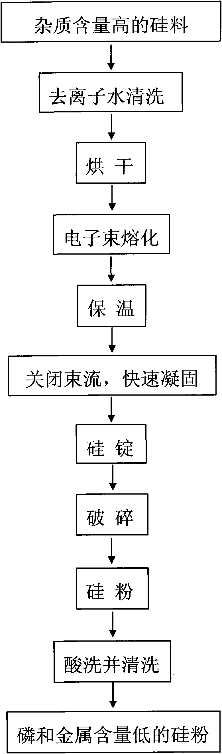
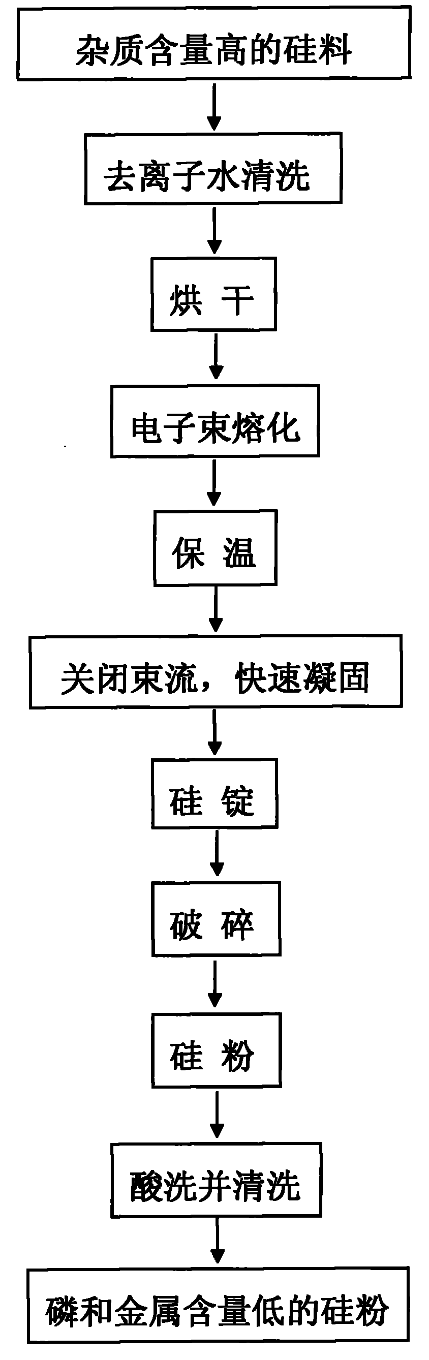
[0018] Electron beam smelting technology is one of the most important methods in the metallurgical preparation of solar-grade silicon. In the process of melting silicon material, electron beams provide high-density energy. After the energy is converted into heat, the temperature of silicon material increases, thereby melting the silicon material. , after complete melting, smelting for a certain period of time, the impurity elements in the silicon melt with a small saturated vapor pressure, such as phosphorus, evaporate into gas and are drawn away; after the volatile impurities are removed, the silicon melt solidifies rapidly, and the crystal The grain size tends to be small, and a large number of metal impurities can become the center of non-uniform nucleation, so the silicon ingot will be composed of many fine grains after solidification, the metal impurities are enriched at the grain boundaries of the grains, and the silicon ingot is broken along the grain boundaries Finally,...


PUM

PropertyMeasurementUnit
particle sizeaaaaaaaaaa

Abstract

The invention relates to a method for extracting polysilicon through electron beams and acid washing, comprising the following steps of: firstly, placing a silicon material containing high impurity content into an electron beam smelting furnace, carrying out electron beam smelting to remove the volatile impurity of phosphorus, coagulating rapidly to form a silicon ingot, in which numerous fine grains are formed and metal impurities are enriched on the grain boundary of the grains, finally crushing the silicon ingot along the grain boundary to fully expose the grain boundary, and then carrying out acid washing to remove the metal impurities to obtain the silicon ingot with lower content of the phosphorous and the metal impurities. By combining electron beam smelting used for removing the volatile impurity of the phosphorus, acid washing used for removing the metal impurities on the grain boundary, and further phosphorus removal as well as utilizing the effect that electron beams rapidly coagulates after smelting to generate fine grains, the invention completes the removal process of the phosphorus and the metal impurities efficiently and rapidly, thereby meeting the operating requirements on solar grade silicon; and moreover, the invention has the remarkable characteristics of high purification efficiency, stable technology, short period, high production efficiency, low energy consumption and low cost.

Description

technical field [0001] The invention belongs to the technical field of purifying polysilicon by physical metallurgy technology, and in particular relates to a method for purifying polysilicon by using electron beam smelting technology and pickling. Background technique [0002] With the rapid development of the photovoltaic industry, there is a worldwide shortage of high-purity polysilicon, the most basic raw material for solar cells. At present, the output of polysilicon can no longer meet the production needs, resulting in a shortage of supply and rising prices. In 2006, the price of polysilicon exceeded 300 US dollars / kg, and in 2007 rose to 360-370 US dollars / kg, and then reached a high price of 400 US dollars / kg. Therefore, the development of low-cost, high-efficiency polysilicon preparation methods is of great significance to the development of the photovoltaic industry. [0003] So far, the world-wide preparation of polysilicon materials for solar cells has formed a ...

Claims


Application Information

Patent Timeline
Patent Type & Authority Applications(China)
IPC IPC(8): C01B33/037
CPCY02P20/10
Inventor 战丽姝董伟谭毅李国斌
Owner DALIAN LONGSHENG TECH CO LTD
Why Eureka
Try Eureka