Novel efficient metallic iridium coordination compound red organic electrophosphorescent material and organic electroluminescent device thereof
A technology of phosphorescent materials and complexes, applied in the direction of luminescent materials, electrical solid devices, electrical components, etc., to achieve the effects of excellent materials, high efficiency, and flexible manufacturing processes
- Summary
- Abstract
- Description
- Claims
- Application Information
AI Technical Summary
Problems solved by technology
Method used
Image
Examples
Synthetic example 1
[0033] Synthesis Example 1: Synthesis of Compound 1
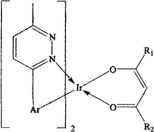
[0034] Compound 1 was synthesized according to the following reaction formula.
[0035]
[0036] Synthesis of intermediate 1a
[0037] Hydrazine hydrate (1.60 g, 31.96 mmol) was added dropwise to a system of levulinic acid (2.32 g, 19.97 mmol) and 80 ml of ethanol while stirring. After the addition was complete, the temperature was raised to reflux, and the reaction was continued for 2 h. Cool to room temperature, and recover ethanol by atmospheric distillation. The residue was cooled to room temperature, and white needle-like crystals were precipitated. The intermediate 1a (1.91g) was obtained by filtration and suction.
[0038] Synthesis of Intermediate 1b
[0039] Slowly add bromine (11.0g, 68.82mmol) dropwise to the system of intermediate 1a (6.60g, 58.81mmol) and 29ml of glacial acetic acid under stirring, and react at 60°C to 70°C for 3 hours after the dropwise addition. Cool to room temperature and place in a...
Embodiment 1
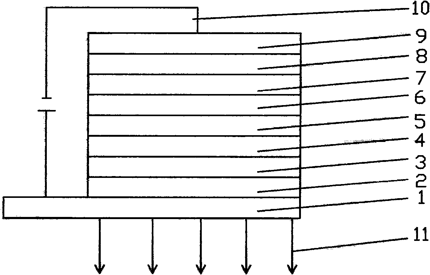
[0051] The embodiment of the present invention selects 7% doping concentration doping, synthesizes the compound 1 in the implementation example 1 as dopant, selects CBP and Zn(BTZ) respectively 2 As the host material of the light-emitting layer, a high-performance electroluminescent device is prepared by thermal evaporation process. The substrate 1 is made of glass or transparent plastic, and the transparent conductive film 2 is a 20Ω / sq ITO (indium tin oxide) film as the anode. 2 Plasma (plasma bombardment) treatment under the atmosphere for 10 minutes, and then in high vacuum (3 ~ 2 × 10 -4 pa), deposit a hole injection layer 3 with a thickness of 45nm on the transparent conductive film 2, and select 2T-NATA; then deposit a hole transport layer 4 on the hole injection layer 3, select NPB, and have a thickness of 25nm; A luminescent layer 5 is deposited on the hole transport layer, and the luminescent layer 5 is co-deposited to evaporate A at the same time, wherein A is CBP ...
Embodiment 2
[0057] In the embodiment of the present invention, the manufacturing process is the same as in embodiment 1, and the light-emitting layer 5 selects Zn (BTZ) 2 Make the light-emitting layer matrix, and synthesize compound 1 in Example 1, its mass ratio is 100: X, wherein x=4, 6, 8, 10, the thickness of the light-emitting layer with different doping concentrations is 25nm;
[0058] When using device structure: ITO / 2T-NATA(45nm) / NPB(25nm) / Zn(BTZ) 2 : Complex 4=100:X, (X=4, 6, 8, 10, 25nm) / BCP(10nm) / Alq 3 (25nm) / LiF(1nm) / Al(200nm) device performance is shown in Table 1:
[0059] Table 1: Performance chart of devices with different concentrations
[0060]
PUM
| Property | Measurement | Unit |
|---|---|---|
| thickness | aaaaa | aaaaa |
| thickness | aaaaa | aaaaa |
| thickness | aaaaa | aaaaa |
Abstract
Description
Claims
Application Information


