Method and structure for reducing grid resistance of power MOSFET (metal oxide semiconductor field-effect transistor)

A power field effect and gate resistance technology, applied in circuits, electrical components, semiconductor devices, etc., can solve problems such as the inability to greatly reduce gate resistance, achieve performance improvement, fast response speed, and reduce gate resistance Effect

Inactive Publication Date: 2011-01-05
SHANGHAI HUA HONG NEC ELECTRONICS
View PDF0 Cites 3 Cited by
  • Summary
  • Abstract
  • Description
  • Claims
  • Application Information

AI Technical Summary

Problems solved by technology

The effect of changing the doping concentration to increase the operating frequency is not ideal, and the gate resistance cannot be greatly reduced.

Method used


Image

  • Method and structure for reducing grid resistance of power MOSFET (metal oxide semiconductor field-effect transistor)
  • Method and structure for reducing grid resistance of power MOSFET (metal oxide semiconductor field-effect transistor)
  • Method and structure for reducing grid resistance of power MOSFET (metal oxide semiconductor field-effect transistor)

Examples


Embodiment Construction

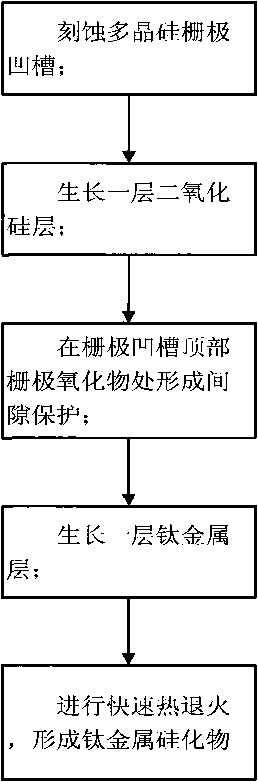
[0016] The method for reducing the gate resistance of a power field effect transistor according to the present invention; comprises the following steps:

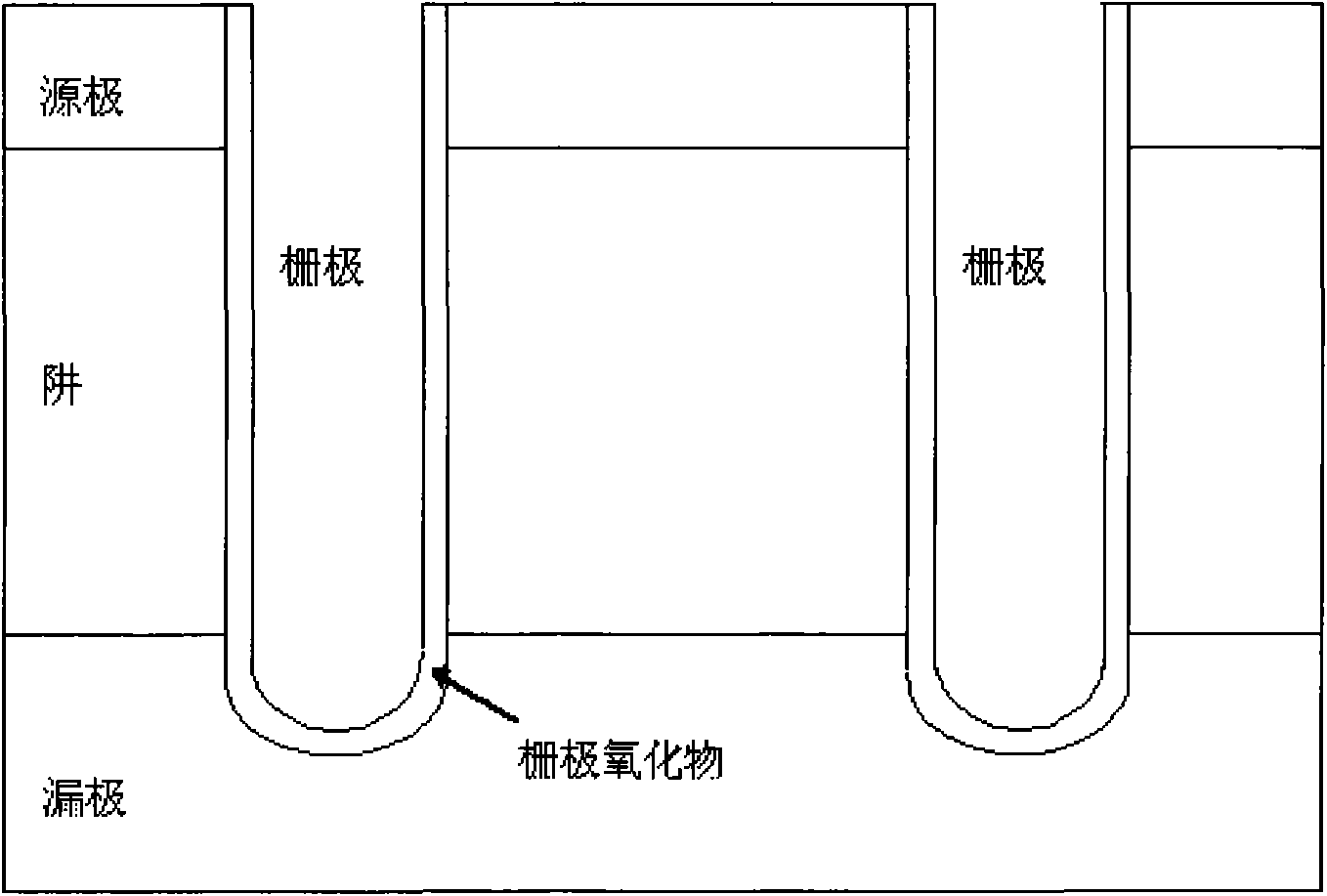
[0017] Step 1. When etching the gate polysilicon, carve out grooves deeper than ordinary power field effect transistors. The depth of the grooves is about 1500-3000 angstroms; Source) ion implantation is performed before; then well (Well) ion implantation and source (Source) ion implantation are performed according to the normal process.

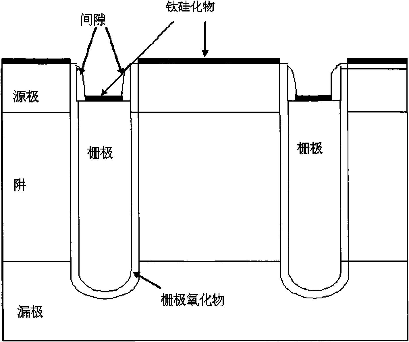
[0018] Compared with the currently known polysilicon gate groove, the structure is basically the same, but the polysilicon gate groove of the present invention is deeper than the polysilicon gate groove of the currently known power MOS device, and this is done to reserve some space Give the titanium metal silicide to be formed below.

[0019] Step 2: After the Well ion implantation and the Source ion implantation are completed as described in Step 1, a layer of silicon dioxide with a cert...


PUM

PropertyMeasurementUnit
thicknessaaaaaaaaaa
thicknessaaaaaaaaaa
thicknessaaaaaaaaaa

Abstract

The invention discloses a method and structure for reducing the grid resistance of a power metal oxide semiconductor field-effect transistor (MOSFET). The method comprises the following steps: etching a polysilicon gate groove; growing a silicon dioxide layer; back-etching the silicon dioxide layer so as to form a clearance protection on gate oxides on the top of the polysilicon gate groove; growing a titanium layer; and carrying out rapid thermal annealing on the titanium layer so as to form titanium silicides. Based on the technology of an original power MOS device, in the invention, the grid resistance is only on the level of metal resistance and the grid resistance of the power MOSFET is reduced without adding additional photo-masks and by increasing little cost and forming the titanium silicides, thereby improving the operating frequency of the power MOSFET, obtaining a power MOSFET with faster response speed and increasing the properties of the power MOSFET greatly.

Description

technical field [0001] The invention relates to the field of semiconductor manufacturing, in particular to a method and structure of a power field effect transistor. Background technique [0002] Before the invention of power field effect transistors, only power bipolar transistors could be used in high speed and medium power range. Power bipolar transistors were invented in the early 1950s. With the continuous improvement of technology, people can manufacture bipolar power transistors with an operating current of hundreds of amperes and a withstand voltage of up to 600 volts. [0003] However, there are some inherent defects in the working performance of bipolar power transistors. First of all, the bipolar power transistor is a current control device, which requires a large base current to ensure its stability in a certain working state, usually 1 / 5 to 1 / 10 of the collector current. Therefore, in order to obtain a high turn-off speed, a larger reverse base drive current i...

Claims


Application Information

Patent Timeline
Patent Type & Authority Applications(China)
IPC IPC(8): H01L21/283H01L29/78H01L29/49
Inventor 严玮彪王凡魏炜
Owner SHANGHAI HUA HONG NEC ELECTRONICS
Why Eureka
Try Eureka