Method for preparing copper nitride film, copper nitride/copper and copper two-dimensional ordered array

A two-dimensional array, copper nitride technology, applied in the direction of ion implantation plating, coating, metal material coating process, etc., can solve the problems of difficult preparation of copper nitride, and achieve the effect of small lateral diffusion

Active Publication Date: 2011-01-19
CHANGZHOU UNIV
View PDF4 Cites 14 Cited by
  • Summary
  • Abstract
  • Description
  • Claims
  • Application Information

AI Technical Summary

Problems solved by technology

Therefore, unlike other nitrides, the preparation of copper nitride is relatively difficult

Method used


Image

  • Method for preparing copper nitride film, copper nitride/copper and copper two-dimensional ordered array
  • Method for preparing copper nitride film, copper nitride/copper and copper two-dimensional ordered array
  • Method for preparing copper nitride film, copper nitride/copper and copper two-dimensional ordered array

Examples


Embodiment 1

[0034] Formation of Copper Nitride Films on Silicon Substrates by Implanting Copper Films with Nitrogen Ions

[0035] 1. Copper film deposited by sputtering

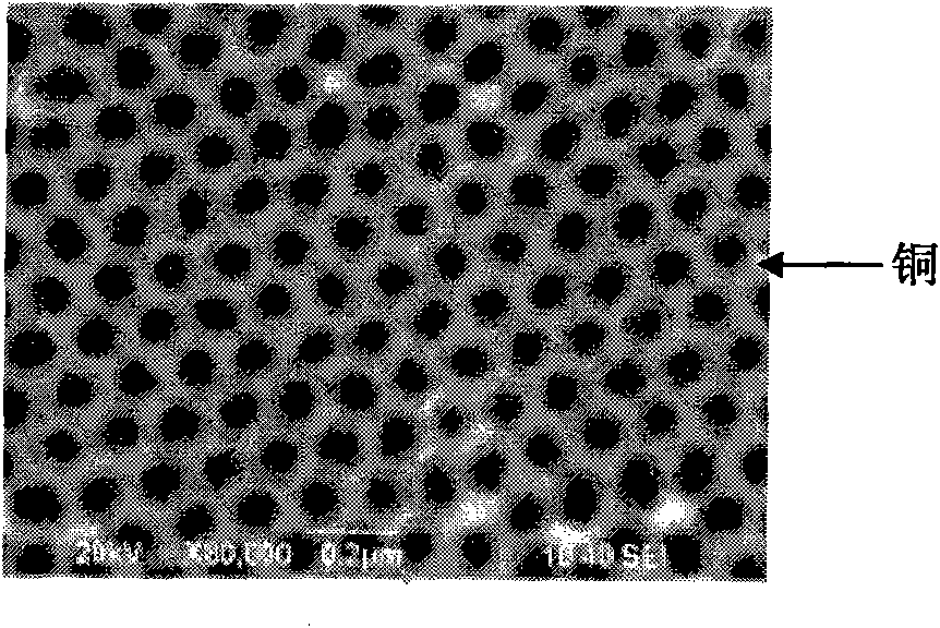
[0036] Silicon is selected as the substrate, the silicon substrate is cleaned by a standard process, and then a 200nm copper film is deposited on the silicon wafer by radio frequency magnetron sputtering.

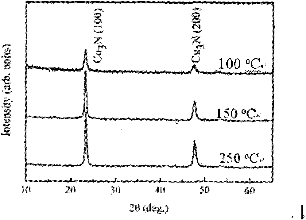
[0037] The background vacuum of the chamber during sputtering is 1×10 -4 Pa, Ar flow rate is 20cm 3 / min, the sputtering pressure is 0.5Pa, the sputtering power is 100W; the distance between the target and the substrate is 6cm. The deposition temperature was 30°C. figure 1 is the XRD pattern of a copper film formed by sputtering on a silicon substrate. The two diffraction peaks in the figure correspond to the (111) and (200) crystal orientations of copper crystals respectively, and have certain preferred orientations. The deposited copper film is polycrystalline.

[0038] 2. Ion implantation of copper film

[0...

Embodiment 2

[0041] Formation of Copper Nitride Films on Silicon Substrates by Implanting Copper Films with Nitrogen Ions

[0042] 1. Copper film deposited by sputtering

[0043] Same as instance 1

[0044] 2. Ion implantation of copper film

[0045] Same as instance 1

[0046] The difference is that the substrate temperature is controlled at 150°C during implantation.

Embodiment 3

[0048] Formation of Copper Nitride Films on Silicon Substrates by Implanting Copper Films with Nitrogen Ions

[0049] 1. Copper film deposited by sputtering

[0050] Same as instance 1

[0051] 2. Ion implantation of copper film

[0052] Same as instance 1

[0053] The difference is that the substrate temperature is controlled at 250°C during implantation.

[0054] figure 2 is the XRD pattern of copper nitride. There is a strong diffraction peak, corresponding to Cu 3 The (100) and (200) crystal orientations of N have no obvious diffraction peaks corresponding to Cu, indicating that a copper nitride film has been formed.


PUM

PropertyMeasurementUnit
thicknessaaaaaaaaaa
pore sizeaaaaaaaaaa
thicknessaaaaaaaaaa

Abstract

The invention discloses a method for preparing a copper nitride film, a copper nitride/copper and copper two-dimensional ordered array, and belongs to the technical field of semiconductor material and micro-nano structure preparation. The method comprises the following steps of: preparing the copper nitride by adopting ion implantation synthesis, growing a layer of copper film on a silicon slice,a silicon dioxide slice, a ceramic slice or a metal substrate by adopting a sputtering method, and forming the copper nitride film by using nitrogen ion implantation; forming the copper nitride/copper two-dimensional array by adopting a prepared uniform ordered anodic aluminum oxide through-hole template as a mask and using nitrogen ion implantation; and corroding the copper nitride/copper two-dimensional array by using a wet corrosion process to obtain an elemental copper hole array. The ion implantation concentration and the ion implantation depth can be accurately controlled by adopting the ion implantation process, and the transverse diffusion is low. The structure of the two-dimensional array and the characteristic dimension of the array can be changed by selecting the proper aluminum oxide template.

Description

technical field [0001] The invention relates to a semiconductor material and a method for preparing a two-dimensional ordered array, in particular to forming a copper nitride thin film by using ion implantation technology, and combining double-pass alumina template technology and ion implantation technology to form a copper nitride / copper two-dimensional The ordered structure can regulate the characteristic size of the two-dimensional array by selecting the appropriate alumina template and implantation process. The invention belongs to the technical field of semiconductor material and micro-nano structure preparation. Background technique [0002] Copper nitride is a semiconductor material with a cubic inverse ReO3 lattice structure, and the lattice constant is 0.382nm. The band gap is about 1.3eV, and it is one of the hottest semiconductor materials currently being studied. At present, the commonly used method for preparing copper nitride (Cu3N) film is sputtering method,...

Claims


Application Information

Patent Timeline
Patent Type & Authority Applications(China)
IPC IPC(8): C23C14/48C23C14/06C23C14/34C23C14/04C23C14/58
Inventor 丁建宁袁宁一丁古巧
Owner CHANGZHOU UNIV
Why Eureka
Try Eureka