First-coating last-etching single package method for positively packaging double-sided graphic chip

A graphics chip and packaging method technology, which is applied in the manufacture of electrical components, electrical solid devices, semiconductor/solid devices, etc., can solve the problems of large volume and area, slow signal output speed of the chip, and high cost of metal wires, and achieve volume and Effects of reduced area, shorter length, and lower cost

Active Publication Date: 2011-01-19
JCET GROUP CO LTD
View PDF4 Cites 10 Cited by
  • Summary
  • Abstract
  • Description
  • Claims
  • Application Information

AI Technical Summary

Problems solved by technology

[0004] In addition, due to the long distance between the chip and the pin, the length of the metal wire is long, such as Figures 45-46 As shown, the cost of metal wires is high (especially expensive pure gold metal wires); also due to the long length of metal wires, the signal output speed of the chip is slow (especially for storage products and those that require a large amount of data) calculation, more prominent); also because the length of the metal wire is longer, the interference of the parasitic resistance / capacitance and the parasitic pole existing in the metal wire to the signal is also higher; and because the chip and the pin between The longer the distance, the larger the volume and area of ​​the package, the higher the material cost, and the more waste

Method used


Image

  • First-coating last-etching single package method for positively packaging double-sided graphic chip
  • First-coating last-etching single package method for positively packaging double-sided graphic chip
  • First-coating last-etching single package method for positively packaging double-sided graphic chip

Examples


Embodiment 1

[0110] Example 1: Single Base Island Single Turn Pin

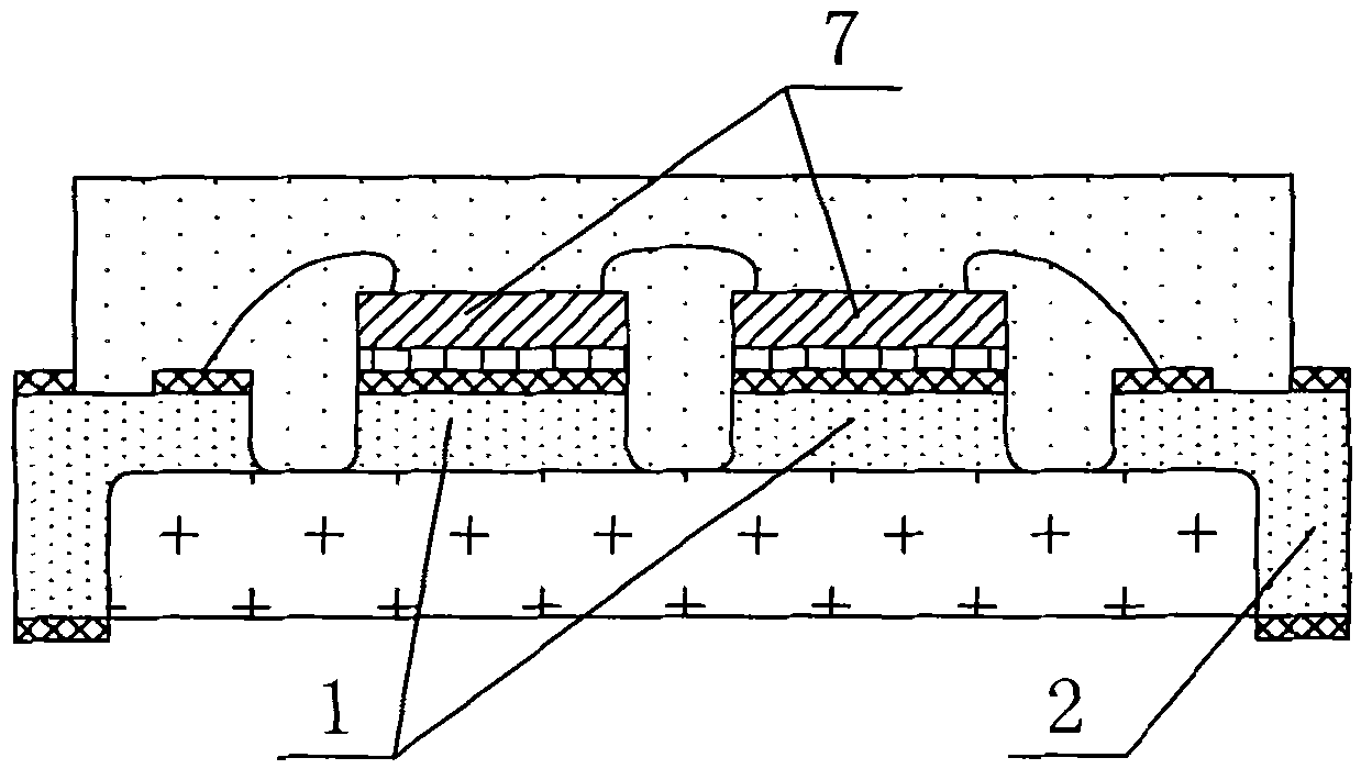
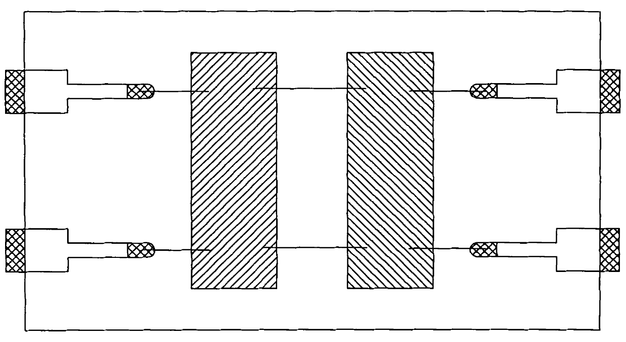
[0111] see figure 2 and image 3 , figure 2 It is a structural schematic diagram of Embodiment 1 of the double-sided graphics chip front-mounted single-chip package structure of the present invention. image 3 for figure 2 top view. Depend on figure 2 and image 3 It can be seen that the double-sided graphic chip of the present invention is mounted on a single package structure, including base island 1, pin 2, plastic encapsulant (epoxy resin) 3 without filler, conductive or non-conductive bonding material 6, chip 7, metal line 8 and filler molding compound (epoxy resin) 9, the front of the pin 2 extends as far as possible to the side of the base island 1, and a first metal layer 4 is arranged on the front of the base island 1 and the pin 2, A second metal layer 5 is arranged on the back side of the base island 1 and pins 2, and a chip 7 is arranged on the first metal layer 4 on the front side of the base island...

Embodiment 2

[0151] Embodiment 2: sunken base island exposed type single-turn pin

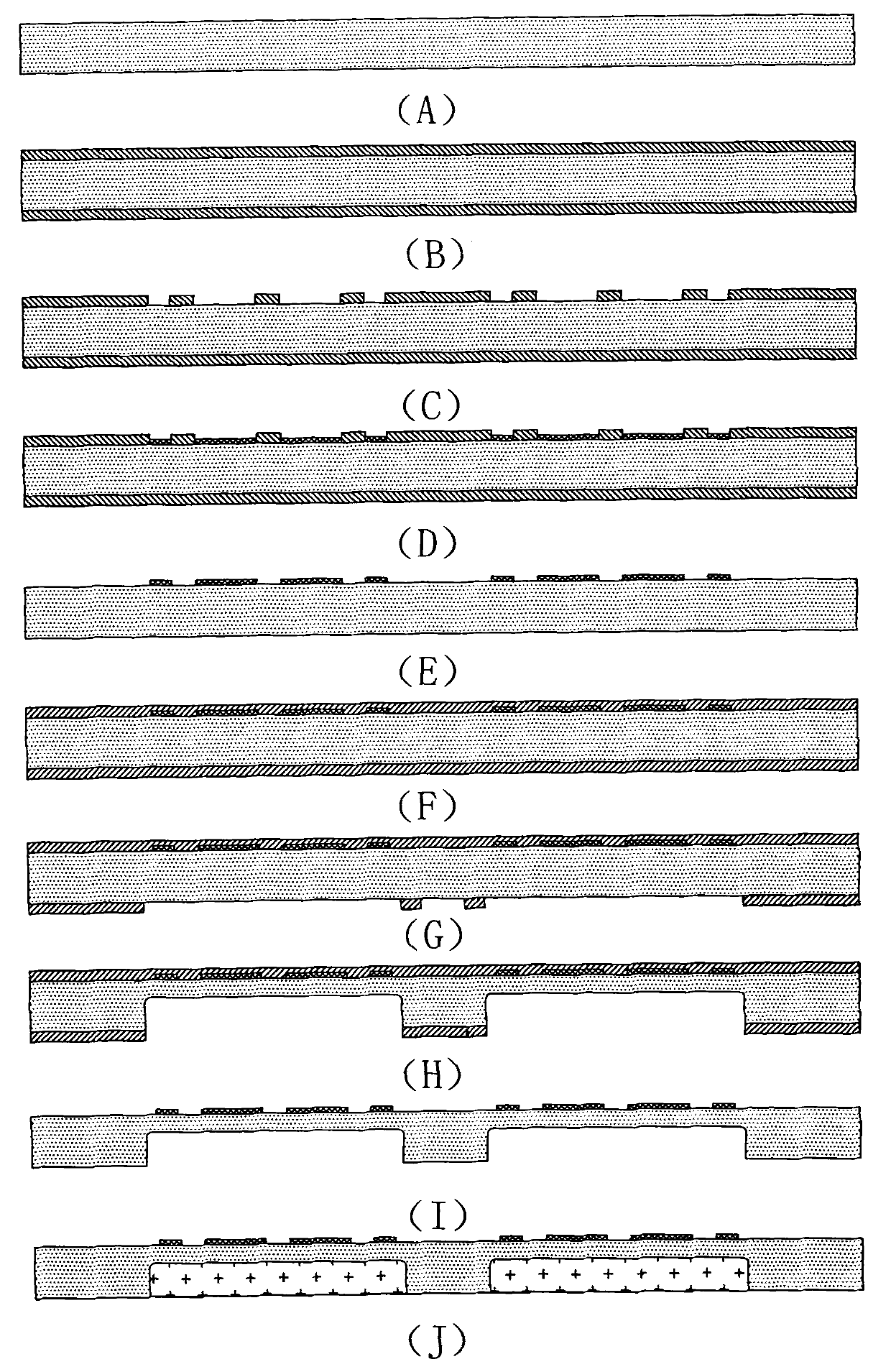
[0152] see Figure 4~6 , Figure 4 (A)~ Figure 4 (R) is a schematic diagram of each process in Embodiment 2 of the double-sided graphics chip packaging method of the present invention, which is first plated and then engraved. Figure 5 It is a structural schematic diagram of Embodiment 2 of the double-sided graphics chip front-mounted single-chip package structure of the present invention. Figure 6 for Figure 5 top view. Depend on Figure 4 , Figure 5 and Figure 6 It can be seen that the only difference between Embodiment 2 and Embodiment 1 is that the base island 1 is a sunken base island, that is, the central area of ​​the front of the base island 1 is sunken.

Embodiment 3

[0153] Embodiment 3: Embedded base island single-turn pin

[0154] see Figure 7-9 , Figure 7 (A)~ Figure 7 (R) is a schematic diagram of each process in Embodiment 3 of the double-sided graphics chip packaging method of the present invention, which is first plated and then engraved. Figure 8 It is a structural schematic diagram of Embodiment 3 of the double-sided graphics chip front-mounted single-chip package structure of the present invention. Figure 9 for Figure 8 top view. Depend on Figure 7 , Figure 8 and Figure 9 It can be seen that the difference between Example 3 and Example 1 is that the base island 1 is an embedded base island, that is, the back of the base island 1 is embedded with the filler-free molding compound (epoxy resin) 3 Inside.


PUM


Abstract

The invention relates to a first-coating last-etching single package method for positively packaging a double-sided graphic chip. The method comprises the following technical steps: taking a metal substrate; plating a metal layer to coat the metal substrate; carrying out backside etching on the metal substrate; enveloping plastic pacing material (epoxy resin) without filler on the backside of the metal substrate; carrying out positive etching on the metal substrate; etching the positive sides of a basic island and a pin, wherein the backside sizes of the basic island and the pin are smaller than the positive sizes of the basic island and the pin to form a basic inland and pin structure with big top and small bottom; loading pieces; routing metal wires; enveloping local units by using plastic pacing material (epoxy resin) with filler on the positive side of the semi-finished product to ensure local unit areas on the positive side of the pin to expose the plastic pacing material (epoxy resin) with filler; plating metal layers on the backsides of the island and the pin and the positive side of the pin for coating; and cutting. The package structure of the chip prepared by the method of the invention does not have the problem of falling feet, and the length of the metal wires is shortened.

Description

(1) Technical field [0001] The invention relates to a single packaging method for a double-sided graphics chip, which is first plated and then engraved. It belongs to the technical field of semiconductor packaging. (2) Background technology [0002] The traditional manufacturing method of the chip packaging structure is: after chemical etching and surface electroplating are carried out on the front side of the metal substrate, the production of the lead frame is completed (such as Figure 43 shown). The backside of the leadframe is etched during the packaging process. This law has the following shortcomings: [0003] Because only half-etching work is done on the front of the metal substrate before plastic sealing, and the plastic sealing material is only half a foot high to cover the pins during the plastic sealing process, so the binding ability between the plastic package and the pins becomes smaller. If the plastic package is considerate When the chip is not very good ...

Claims


Application Information

Patent Timeline
Patent Type & Authority Applications(China)
IPC IPC(8): H01L21/50H01L21/48
CPCH01L2224/92247H01L24/97H01L2224/32257H01L2224/48137H01L2224/97H01L2224/73265H01L2224/32245H01L2224/48247H01L24/73H01L2924/00012H01L2224/85H01L2924/00
Inventor 王新潮梁志忠
Owner JCET GROUP CO LTD
Why Eureka
Try Eureka