Method for forming die bonding connection structure of reflective LED at low temperature

A technology for light-emitting diodes and bonding structures, applied in electrical components, circuits, semiconductor devices, etc., can solve problems such as low productivity, damage to light-emitting diode chips, and excessive growth of intermetallic compounds.

Active Publication Date: 2011-01-19
IND TECH RES INST
View PDF0 Cites 5 Cited by
  • Summary
  • Abstract
  • Description
  • Claims
  • Application Information

AI Technical Summary

Problems solved by technology

However, compared with silver colloidal die bonding, the die bonding equipment is more complicated and expensive (the die bonding machine needs to be equipped with a temperature control system and a pressure system), and the production capacity is also lower.
However, if high melting point metal soldering materials are used, such as gold tin (AuSn), gold silicon (AuSi), tin silver (SnAg), tin (Sn), etc., the light-emitting diode chip will be easily damaged due to high junction temperature ( Thermal stress due to difference in thermal expansion coefficient)
If you use low melting point metals, such as indium (In), indium silver (InAg), indium gold (InAu), bismuth tin (BiSn), etc. (about 70-80°C), due to the low melting point of the bonding layer, the material of the bonding layer will soften due to the rapid diffusion of atoms or the phenomenon of excessive growth of intermetallic compounds will occur, resulting in a significant decrease in the reliability of the joint decline

Method used


Image

  • Method for forming die bonding connection structure of reflective LED at low temperature
  • Method for forming die bonding connection structure of reflective LED at low temperature
  • Method for forming die bonding connection structure of reflective LED at low temperature

Examples


Embodiment Construction

[0025] In order to enable your examining committee members to have a further understanding and understanding of the characteristics, purpose and functions of the present invention, a detailed description is given below with the accompanying drawings.

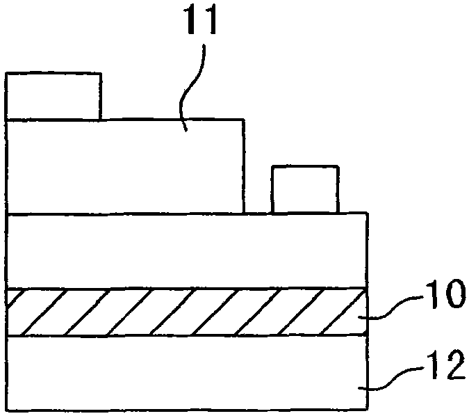
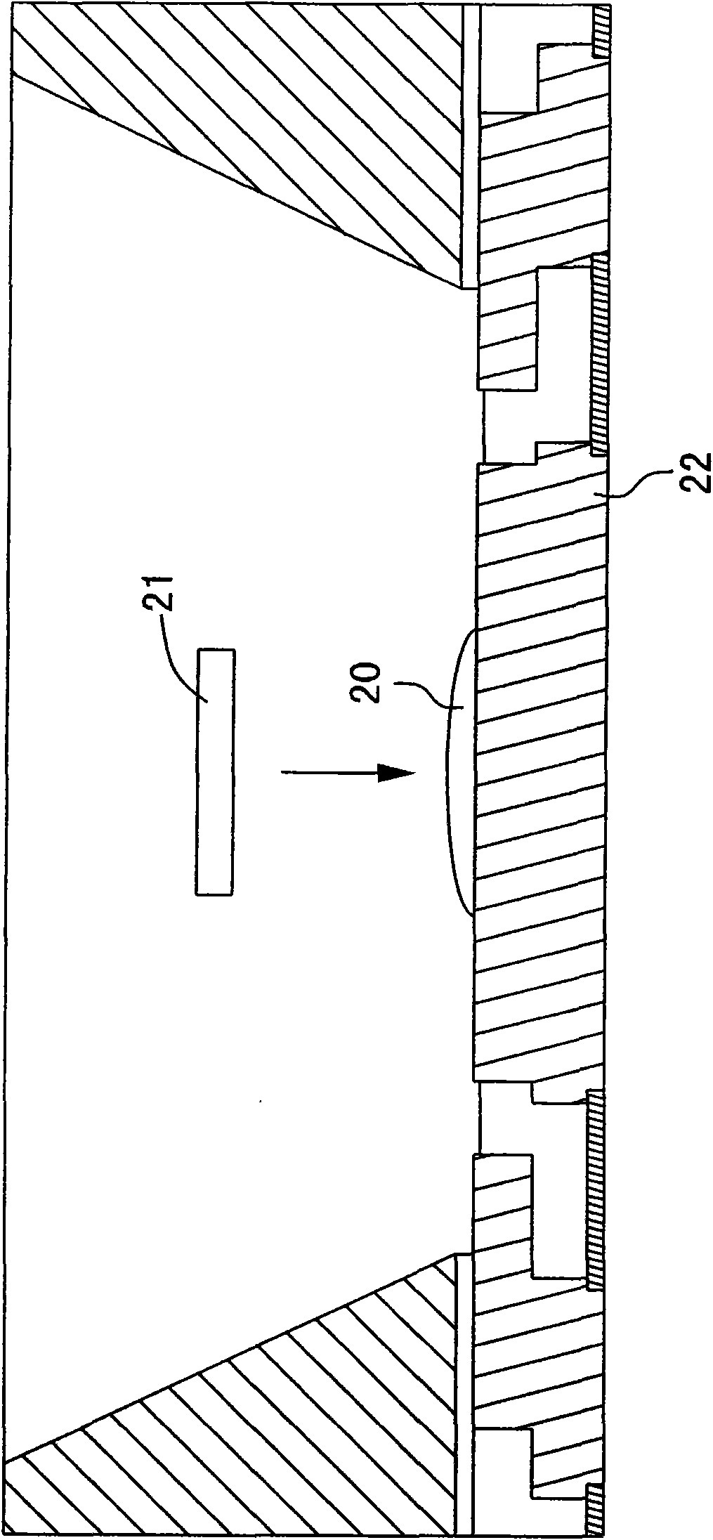
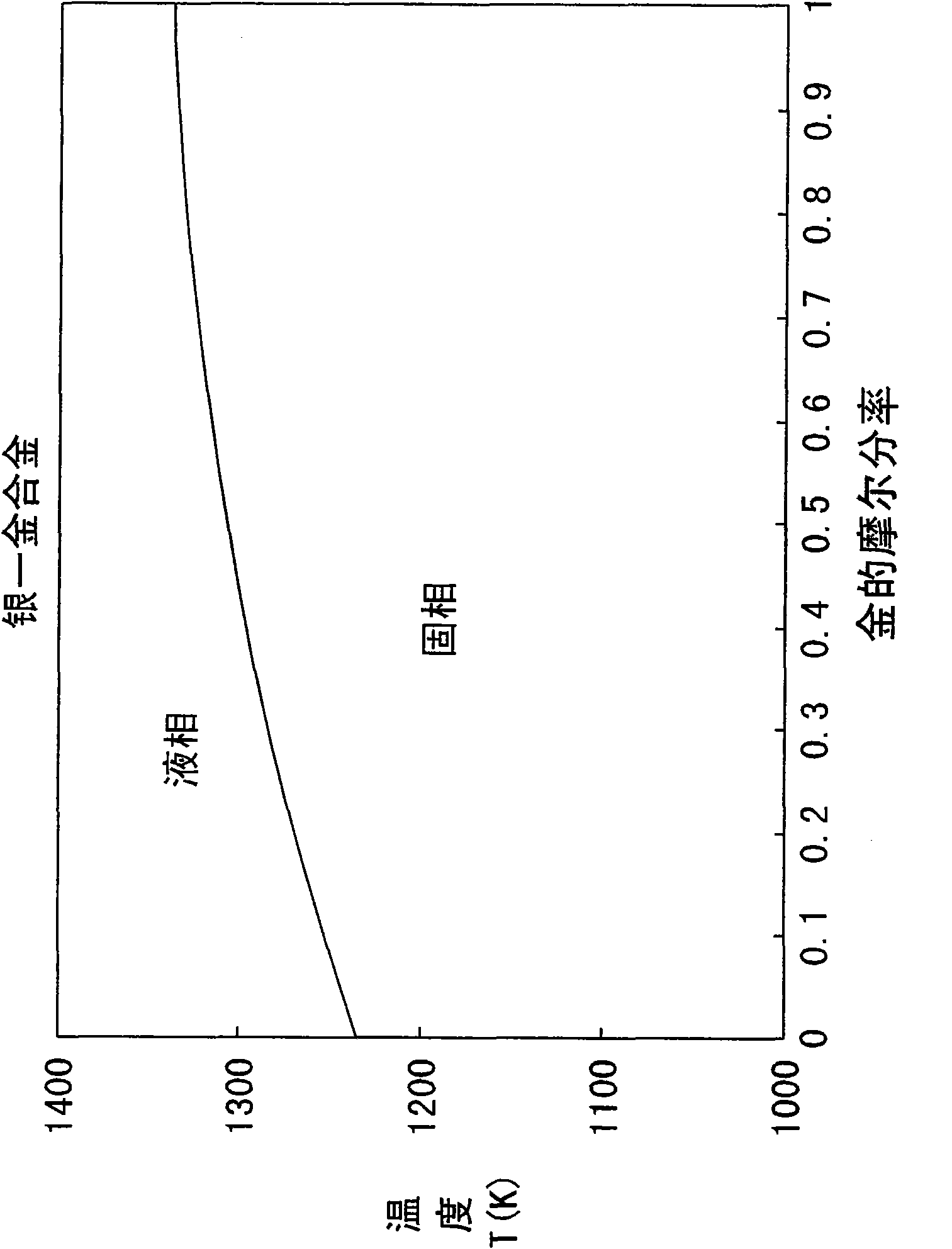
[0026] In view of the shortcomings of the LED die bonding in the prior art, the present invention mainly utilizes the fast diffusion characteristics of the gold / silver interface to achieve the goal of low temperature die bonding, which will avoid different substrates due to different coefficients of thermal expansion (CTE) caused by thermal stress. Since the gold / silver bonding layer is mainly bonded as a metal bond, and by image 3 The gold-silver phase diagram shows that the melting point of the solid solution formed by diffusion is at least as high as 1200K. This joint structure will have the characteristics of high joint strength, high heat dissipation and high temperature resistance. Take the area as 1mm 2 Taking chips as ...


PUM

PropertyMeasurementUnit
thicknessaaaaaaaaaa
thicknessaaaaaaaaaa
melting pointaaaaaaaaaa

Abstract

The invention discloses a method for forming a die bonding connection structure of a reflective LED at low temperature, which comprises the following steps of: forming a first metal layer on a first surface of a base plate, and providing an LED epitaxial structure on a second surface of the base plate; forming a second metal layer on a base body, wherein the material of the second metal layer is different from that of the first metal layer; applying a force to the base plate and the base body so that the first metal layer and the second metal layer produce plastic deformation and are primarily bonded together; and heating the base plate and the base body in a high temperature furnace, wherein the first metal layer and the second metal layer are subjected to solid state diffusion in an interface to form a diffusion alloy layer.

Description

technical field [0001] The invention relates to a method for forming a reflective light-emitting diode crystal bonding structure at low temperature, in particular to a method for utilizing the physical characteristics of rapid diffusion of the gold / silver interface to achieve the goal of low temperature crystal bonding to avoid thermal expansion of different substrates A low-temperature method for forming a reflective light-emitting diode die-bonding structure due to thermal stress problems caused by different coefficients (CTE). Background technique [0002] Since light emitting diodes have the advantages of small size, high luminous efficiency, long life and rich color changes, it is expected that the applications of light emitting diodes will increase. Generally speaking, bare LED chips need to undergo packaging steps such as die bonding, wire bonding, glue sealing, and product classification before the chips can be commercialized to customers. The existing die-bonding m...

Claims


Application Information

Patent Timeline
Patent Type & Authority Applications(China)
IPC IPC(8): H01L33/00
Inventor 林修任林建宪赖杰隆
Owner IND TECH RES INST
Why Eureka
Try Eureka