Biochip and preparation method thereof

A biochip and silicon wafer technology, applied in the field of microelectromechanical systems and cell biology, can solve the problems of cell function, adverse effects of state, increase the number of digestions, cell damage, etc., to reduce the number of cell digestions, improve separation efficiency, and reduce consumption short time effect

Inactive Publication Date: 2011-02-02
TSINGHUA UNIV +1
View PDF4 Cites 15 Cited by
  • Summary
  • Abstract
  • Description
  • Claims
  • Application Information

AI Technical Summary

Problems solved by technology

[0006] 2. The differential digestion method increases the number of digestions, which will cause additional damage to the cells
This process takes

Method used


Image

  • Biochip and preparation method thereof
  • Biochip and preparation method thereof
  • Biochip and preparation method thereof

Examples


Embodiment 1

[0080] Embodiment 1: process centrifugal separator and concentrator on silicon chip

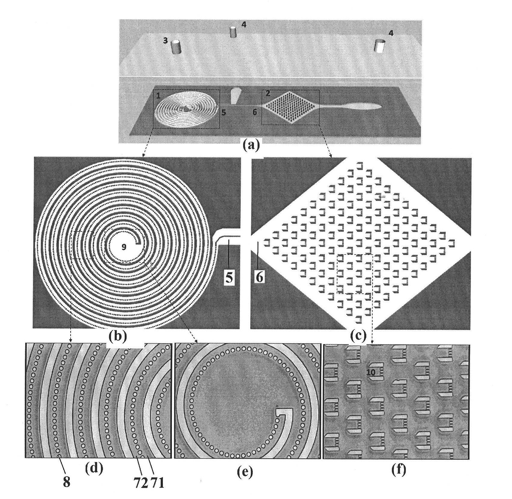
[0081] The structure of this embodiment refers to the attached figure 1 , see the appendix for the process flow figure 2 .

[0082] 1) Process flow of the silicon chip structure of the separator and concentrator:

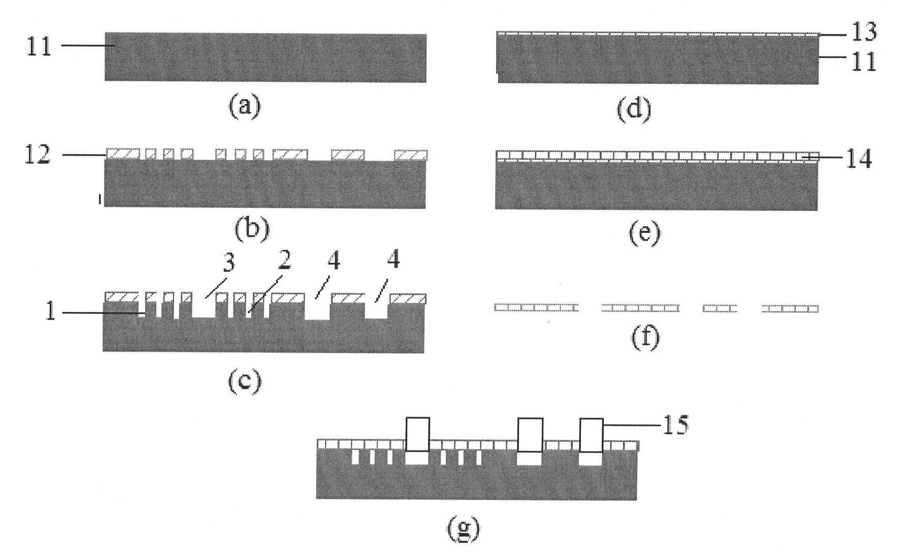
[0083] (a) processing and cleaning the silicon wafer 11;

[0084] (b) Spin glue 12 on the front side of the silicon wafer, pre-baking, photolithography, developing, and post-baking;

[0085] (c) In-depth etching (ICP) of about 100 μm silicon on the front side of the silicon wafer to form a microfluidic channel, a microcolumn array separator 1, a sample inlet 3, an array of concentrators 2, and two sample outlets and sample discharge outlets 4;

[0086] 2) Process flow of cover sheet polymer for separator and concentrator:

[0087] (d) process and clean the silicon wafer 11, and apply a release agent 13 on its surface;

[0088] (e) Pour the bubble-free silicone rubber (PDMS) ...

Embodiment 2

[0091] Example 2: Fabrication of centrifugal separators and concentrators from polymers

[0092] The structure of this embodiment refers to the attached figure 1 , see the appendix for the process flow image 3 .

[0093] 1) Process flow of polymer structure of separator and concentrator:

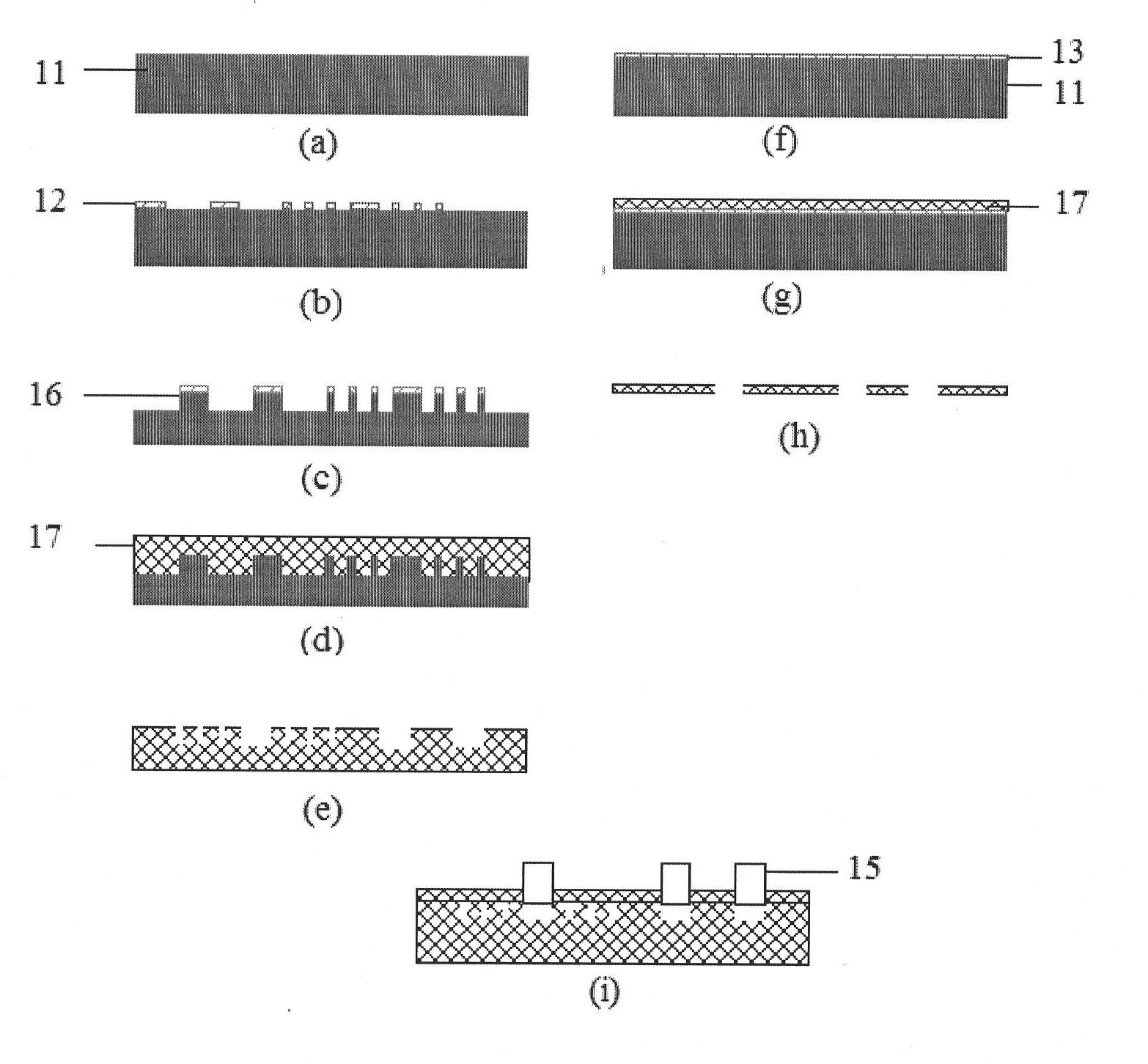
[0094] (a) processing and cleaning the silicon wafer 11;

[0095] (b) Spin glue 12 on the front side of the silicon wafer, pre-baking, photolithography, developing, and post-baking;

[0096] (c) In-depth etching (ICP) of about 100 μm of silicon on the front side of the silicon wafer to form a mold 16 for microfluidic channels, microcolumn array separators and enricher arrays;

[0097] (d) Treat and clean the silicon structure mold, and apply a release agent on its surface, pour the bubble-free PDMS17 on the silicon structure mold, let it stand for flattening, and then bake it in an oven at 60-100°C About 0.5-1 hour, preferably 60°C, 80°C and 100°C;

[0098] (e) peel off the cured PDMS f...

Embodiment 3

[0104] Example 3: Centrifugal Separator and Concentrator of Sandwich Structure

[0105] The structure of this embodiment refers to the attached figure 2 , see the appendix for the process flow Figure 4 .

[0106] (a) processing and cleaning the silicon wafer 11;

[0107] (b) Spin glue 12 on the front side of the silicon wafer, pre-baking, photolithography, developing, and post-baking;

[0108] (c) In-depth etching (ICP) of about 50 μm of silicon on the front side of the silicon wafer to form a microfluidic channel, a microcolumn array separator, a sample inlet, a concentrator array, and two sample outlets (similar to method 1 in structure);

[0109] (d) the front side of the silicon wafer is anodically bonded to the glass 18;

[0110] (e) Thinning the silicon wafer on the back side of the silicon glass sheet after bonding, the method of dry method, wet method or CMP can be adopted;

[0111] (f) Spin glue on the back of the silicon wafer, pre-baking, photolithography, de...


PUM


Abstract

The invention discloses a biochip and a preparation method thereof. The biochip comprises a centrifugal separator, an enricher and an injection port, wherein, the centrifugal separator and the enricher are respectively provided with a discharge port; the centrifugal separator is provided with a centrifugal separator outlet, the enricher is provided with an enricher inlet, and the centrifugal separator outlet is connected with the enricher inlet; the centrifugal separator comprises a vortex microfluid channel and a plurality of micro- columns arranged in the microfluid channel along the fluid flow direction; and the micro- columns divide the microfluid channel into an inner flow channel and an outer flow channel. The biochip of the invention has the advantages of compact structure, reducedtotal area of the biochip, improved separation efficiency, short separation and enrichment process, supported in situ culture and reduced cell dissociation times; and the biochip can also be used forseparating other functional particles.

Description

technical field [0001] The invention relates to the technical fields of micro-electromechanical systems (MEMS) and cell biology, in particular to a biochip and a preparation method thereof. Background technique [0002] Biology-Micro Electromechanical System (Bio-MEMS) technology, which combines biotechnology and MEMS technology, can realize continuous analysis of discontinuous analysis processes in life science research (such as sample preparation, chemical reaction and analysis detection). , integration, and miniaturization, so as to obtain the so-called micro-full analysis system. The system includes sample injection, separation, reaction and detection. In a broad sense, the system also involves transportation. Its ultimate goal is to realize full chemical analysis on the microchip, so as to replace all the functions of conventional analytical laboratories. Compared with traditional instruments, the micro-total analysis system has many advantages such as small size, ligh...

Claims


Application Information

Patent Timeline
IPC IPC(8): C12M3/00
Inventor 杜婧耿照新杨春王玮李志宏
Owner TSINGHUA UNIV
Why Eureka
Try Eureka