
150V-BCD (Binary-Coded Decimal) bulk silicon manufacturing technology and LCD (Liquid Crystal Display) backlight drive chip

A 150V-BCD, manufacturing process technology, applied in semiconductor/solid-state device manufacturing, instruments, electrical components, etc., can solve the problems of limiting the application of LCD high-voltage drive technology, high LED cost, and increasing cost expenses, so as to improve chip yield , reduce chip prices, optimize the effect of charge distribution

Inactive Publication Date: 2012-09-26
WUXI JINGKAI TECH
View PDF0 Cites 1 Cited by
  • Summary
  • Abstract
  • Description
  • Claims
  • Application Information

AI Technical Summary

Problems solved by technology

Although advanced LED backlight technology has been recognized by the industry as the next generation of new backlight display technology, factors such as high LED cost and immature technology limit its application at this stage.
[0003] At present, the field-induced light source EL with capacitive load characteristics is mostly driven by the SOI high-voltage process technology with good electrical isolation and high cost.
In order to meet consumers' desire for rich colors, vivid and high-quality display effects, the number of channels of the high-voltage driver chip needs to be increased to more than 8, which will greatly increase the cost and expenditure, which limits the application of LCD high-voltage driver technology

Method used


Image

  • 150V-BCD (Binary-Coded Decimal) bulk silicon manufacturing technology and LCD (Liquid Crystal Display) backlight drive chip
  • 150V-BCD (Binary-Coded Decimal) bulk silicon manufacturing technology and LCD (Liquid Crystal Display) backlight drive chip
  • 150V-BCD (Binary-Coded Decimal) bulk silicon manufacturing technology and LCD (Liquid Crystal Display) backlight drive chip

Examples


Embodiment Construction

[0055] The BCD process development and EL driver chip design involved in the present invention will be further described below in conjunction with the accompanying drawings and examples.

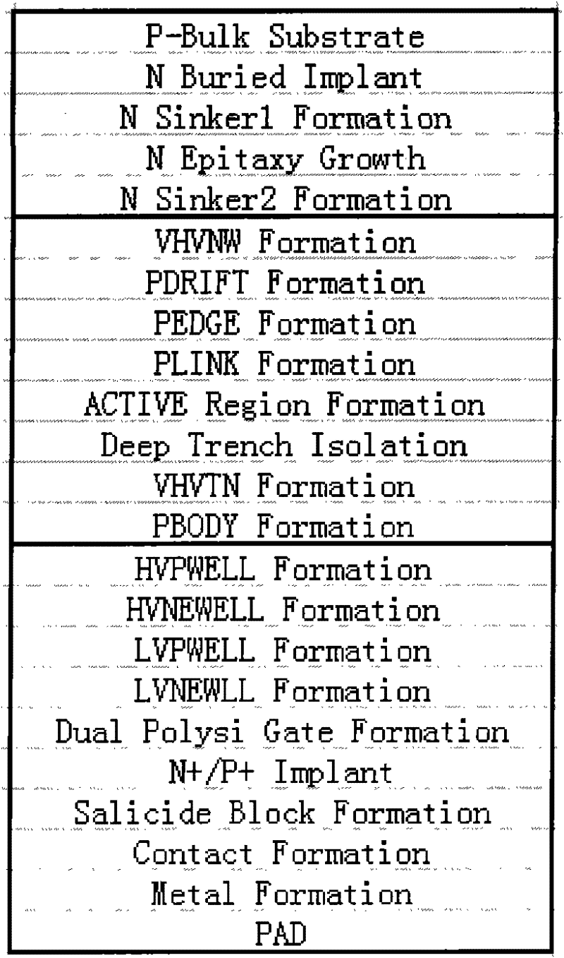
[0056] figure 1 and figure 2 The specific scheme of developing 150V-BCD technology and devices is expounded. The BCD main process has a total of 24 steps, which reduces the LDPMOS two photolithography (thick gate oxide, auxiliary drift region), one implant (auxiliary drift region) and one oxidation compared with the typical BCD process. First, prepare a high-resistivity P-type substrate silicon wafer, implant high-energy ions into Sb to form an N-type buried layer, ion-implant phosphorus element P, and arsenic element As and drive them in at high temperature to form a drain pair connected to the N-type buried layer. NSINKER1 structure, epitaxial N-type epitaxial layer that can meet the Double-Resurf withstand voltage requirements, ion implantation of phosphorus element P, arsenic element ...


PUM


Abstract

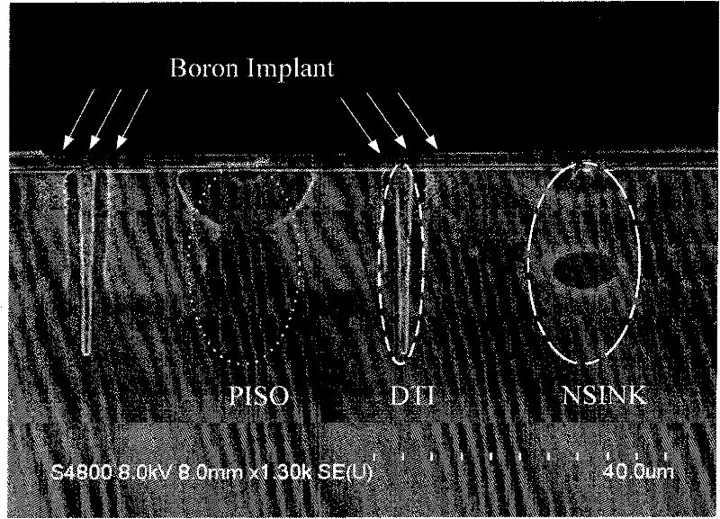
The invention discloses a 150V-BCD (Binary-Coded Decimal) bulk silicon manufacturing technology and an LCD (Liquid Crystal Display) backlight drive chip. The 150V-BCD bulk silicon manufacturing technology comprises the following steps of: preparing a high-resistance substrate silicon sheet; adding an N-shaped buried layer on a substrate; connecting the N-shaped buried layer by using an NSINKER1 drain structure; extending an N-shaped extension layer; forming an opposite-pass structure with NSINKER2; forming an LDPMOS device region, a Resurf voltage resisting region and a channel connecting region to form a horizontal structure LPMOS high- voltage device; forming a Resurf voltage resisting region, a compensation injection JFET region, a VDNMOS device region and a composite MOS (Metal-Oxide Semiconductor) gate channel; replacing the traditional PISO isolation structure by using a deep-groove isolation structure; using double thin gate oxide (DGO) as gate oxide of a low voltage device; using N+ / P+ as drain injection of all devices; reducing interconnection resistance by using a self-alignment silicide technology (Salicide); forming contact holes; forming device connection by using MET; and using press welding points by using PAD. The LCD backlight drive chip comprises a multilevel charge-pump voltage booster circuit, an EL oscillating circuit, a VSENSE module, a high-voltage conversion module and a full-bridge type drive structure.

Description

technical field [0001] The invention relates to a 150V-BCD bulk silicon manufacturing process and an LCD backlight drive chip, and belongs to the technical field of 150V-BCD process development and LCD high-voltage power chips. Background technique [0002] With the rapid development of semiconductor microelectronics technology and liquid crystal display technology in recent decades, the application of portable LCD electronic products has been recognized by consumers and widely used. The field EL light source that provides backlight display for LCD is currently the mainstream display technology due to its advantages of compact size, uniform light output, and low power consumption. Although advanced LED backlight technology has been recognized by the industry as the next generation of new backlight display technology, factors such as high cost of LED and immature technology limit its application at this stage. [0003] At present, the field-induced light source EL with capac...

Claims


Application Information

Patent Timeline
Patent Type & Authority Patents(China)
IPC IPC(8): H01L21/8249H01L21/762G09G3/36
Inventor 黄伟徐湘海王胜万清胡南中
Owner WUXI JINGKAI TECH
Learn More