Method for manufacturing lattice graded buffer layer

A technology of graded buffer layer and graded layer, applied in the field of semiconductor, can solve the problems such as the inability to eliminate mismatch, the high density of threading dislocations on the surface of the structure and the device, the influence of the interface material of the heterojunction material and the performance of the device, etc. Achieve the effect of reducing dependence, overcoming performance degradation, and controlling defect density

Active Publication Date: 2011-04-13
CHINA ELECTRONIC TECH GRP CORP NO 18 RES INST +1
View PDF3 Cites 10 Cited by
  • Summary
  • Abstract
  • Description
  • Claims
  • Application Information

AI Technical Summary

Problems solved by technology

However, due to the existence of residual compressive strain in the graded layer, the lattice constant of the surface of the graded layer is usually smaller than the lattice constant to be controlled, so the threading dislocation density on the surface of the structure and device is still very large, which cannot be well eliminated The impact of mismatch; at the same time, when the top material of the graded layer is different fr

Method used


Image

  • Method for manufacturing lattice graded buffer layer
  • Method for manufacturing lattice graded buffer layer

Examples


preparation example Construction

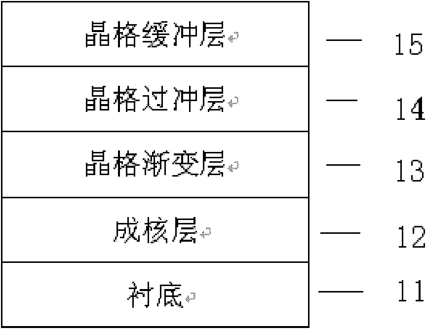
[0025] A preparation method of a lattice gradient buffer layer, the steps are:

[0026] Step (1): use germanium (Ge) single crystal as the substrate 11; the substrate material can be germanium, silicon, and III-V and II-VI group materials or their combination, including gallium arsenide, indium phosphide , gallium phosphide, gallium nitride, gallium antimonide, etc.; the substrate surface may have (100), (110) or (111) crystallographic directions, or other index plane directions, as well as directions in other directions including the above directions 0-15 degree deflection angle.

[0027] Step (2): Utilize existing epitaxy techniques such as metal organic chemical vapor deposition (MOCVD), molecular beam epitaxy (MBE) and liquid phase epitaxy (LPE), carry out the epitaxial growth of material; In order to make the core functional layer of the present invention application— —The structure of the lattice gradient buffer layer is not affected by the defects of the substrate. Fir...


PUM


Abstract

The invention relates to a method for manufacturing a lattice graded buffer layer, which comprises the following steps of: (1) using a commercial germanium single crystal, arsenide gallium single crystal or indium phosphide single crystal as a substrate; (2) epitaxially forming a layer of material in lattice matching with the substrate material as a nucleation layer by utilizing epitaxial technology; (3) epitaxially growing a lattice graded layer on the nucleation layer until the lattice of the material of a top layer has an ideal lattice constant or a lattice constant slightly lower than theideal lattice constant, wherein the lattice graded layer consists of a plurality of indium gallium arsenide materials with gradually increased components; (4) epitaxially forming a layer of indium gallium arsenide material with the lattice constant more than the ideal lattice constant on the lattice graded layer as a lattice overshoot layer; and (5) epitaxially forming a layer of material which has the lattice constant equal to the ideal lattice constant and is the same as that grown on an adjacent upper layer thereof as the lattice buffer layer. The method solves the problem of influence of device appearance degradation caused by lattice mismatching between a conventional epitaxial material and the substrate, and can effectively control threading dislocation density on the surface of a device.

Description

technical field [0001] The invention belongs to the technical field of semiconductors, and relates to a structure and a manufacturing method of a semiconductor device, in particular to a preparation method of a lattice gradient buffer layer. Background technique [0002] Since the 1970s, with the gradual development and maturity of epitaxial equipment such as liquid phase epitaxy (LPE), metal organic chemical vapor deposition (MOCVD) and molecular beam epitaxy (MBE), various semiconductor devices today are produced in various prepared by epitaxial growth on a commercially available epitaxial substrate. This growth method determines that in most cases, the epitaxial material must maintain a lattice match with the epitaxial substrate, otherwise internal stress will be generated due to lattice mismatch, resulting in a lot of misfit dislocations and penetrations inside the crystal. Dislocation. Because dislocations destroy the translational symmetry of the crystal, a large num...

Claims


Application Information

Patent Timeline
IPC IPC(8): C30B25/16
Inventor 刘如彬王帅孙强孙彦铮
Owner CHINA ELECTRONIC TECH GRP CORP NO 18 RES INST
Why Eureka
Try Eureka