TFT-LCD array substrate and manufacturing method thereof
An array substrate and substrate technology, applied in the field of TFT-LCD array substrate and its manufacturing, can solve the problems of immature process technology and high production cost, and achieve the goal of eliminating step defects, improving yield, and reducing feedthrough voltage Effect
- Summary
- Abstract
- Description
- Claims
- Application Information
AI Technical Summary
Problems solved by technology
Method used
Image
Examples
preparation example Construction
[0079] (5) The present invention adopts the existing mature preparation technology, the process changes little, not only the production cost is low, but also the product quality can be guaranteed, and has wide application prospect.
[0080] It should be noted that the above technical solution is only a structural form of the TFT-LCD array substrate of the present invention, and in practical application, similar or similar structures can be formed by changing materials or adjusting process flow. For example, the coating of the color resin layer and the black matrix of the present invention can be deposited by means of inkjet or the like. For another example, the aforementioned third patterning can be completed through a secondary patterning process using a common mask.
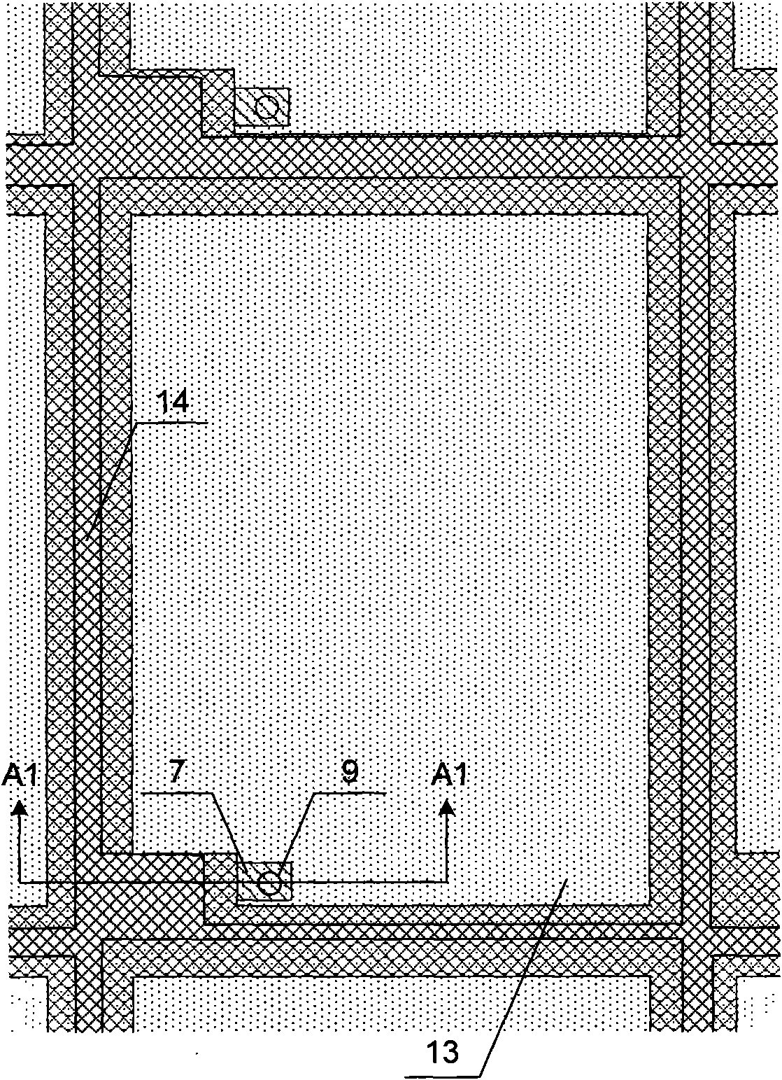
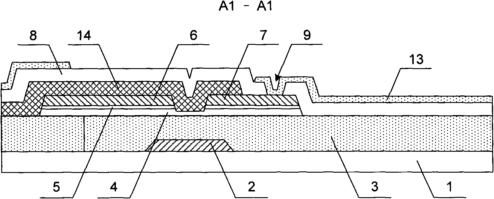
[0081] Figure 13 It is a schematic diagram of another structural form of the TFT-LCD array substrate of the present invention, which is figure 1 Sectional view of A1-A1 in the middle. This embodiment is a m...
no. 3 example
[0113] exist Figure 16 On the basis of the technical solution of the illustrated embodiment, the third embodiment of the TFT-LCD array substrate manufacturing method of the present invention can also be formed by canceling the passivation layer, including:
[0114] Step 31, using magnetron sputtering or thermal evaporation to deposit a gate metal film on the substrate, and using a common mask to form a pattern including gate electrodes and gate lines through a patterning process;
[0115] Step 32, forming a colored resin layer composed of a red resin pattern, a blue resin pattern and a green resin pattern, and the thickness of the colored resin layer used as an insulating layer is 1.5 μm to 3 μm;
[0116] Step 33, using the plasma-enhanced chemical vapor deposition method to sequentially deposit the semiconductor film and the doped semiconductor film; using magnetron sputtering or thermal evaporation to deposit the source-drain metal film;
[0117] Step 34, coating a layer o...
no. 4 example
[0121] exist Figure 17 On the basis of the technical solution of the illustrated embodiment, the fourth embodiment of the TFT-LCD array substrate manufacturing method of the present invention can also be formed by canceling the passivation layer, including:
[0122] Step 41, using magnetron sputtering or thermal evaporation to deposit a gate metal film on the substrate, and using a common mask to form a pattern including gate electrodes and gate lines through a patterning process;
[0123] Step 42, forming a colored resin layer composed of a red resin pattern, a blue resin pattern and a green resin pattern, and the thickness of the colored resin layer used as a gate insulating layer is 1.5 μm to 3 μm;
[0124] Step 43, using a plasma-enhanced chemical vapor deposition method to sequentially deposit a semiconductor thin film and a doped semiconductor thin film;
[0125] Step 44, using a common mask to form a pattern including the active layer through a patterning process;
...
PUM
| Property | Measurement | Unit |
|---|---|---|
| Layer thickness | aaaaa | aaaaa |
Abstract
Description
Claims
Application Information
 - R&D
- Intellectual Property
- Life Sciences
- Materials
- Tech Scout
- Unparalleled Data Quality
- Higher Quality Content
- 60% Fewer Hallucinations
Browse by: Latest US Patents, China's latest patents, Technical Efficacy Thesaurus, Application Domain, Technology Topic, Popular Technical Reports.
© 2025 PatSnap. All rights reserved.Legal|Privacy policy|Modern Slavery Act Transparency Statement|Sitemap|About US| Contact US: help@patsnap.com


