Glue spraying processing device used in semiconductor manufacturing

A processing device and semiconductor technology, which is applied to liquid injection devices, devices for processing microstructures, devices for coating liquids on surfaces, etc., can solve problems such as inability to meet manufacturing requirements, achieve simple and ingenious structures, and ensure uniformity

Inactive Publication Date: 2011-04-20
SHENYANG KINGSEMI CO LTD
View PDF2 Cites 18 Cited by
  • Summary
  • Abstract
  • Description
  • Claims
  • Application Information

AI Technical Summary

Problems solved by technology

[0002] Part of the bump packaging process requires that a photoresist or a protective isolation layer be coated on the surface of the wafer with a highly undulating surface or a wafer with deep holes. This isolation layer requires uniform thickness at all points, whether it is at the corner of the slope. Consistent, while the traditional glue drop spin coating process can only fill up the undulations or deep holes to form a plane, because the coating thickness of each point is different, resulting in various defects in the subsequent manufacturing process and cannot meet the manufacturing requirements. requirements, which cannot be achieved by spin coating

Method used


Image

  • Glue spraying processing device used in semiconductor manufacturing
  • Glue spraying processing device used in semiconductor manufacturing
  • Glue spraying processing device used in semiconductor manufacturing

Examples


Embodiment Construction

[0024] The present invention will be further described below in conjunction with the accompanying drawings and embodiments.

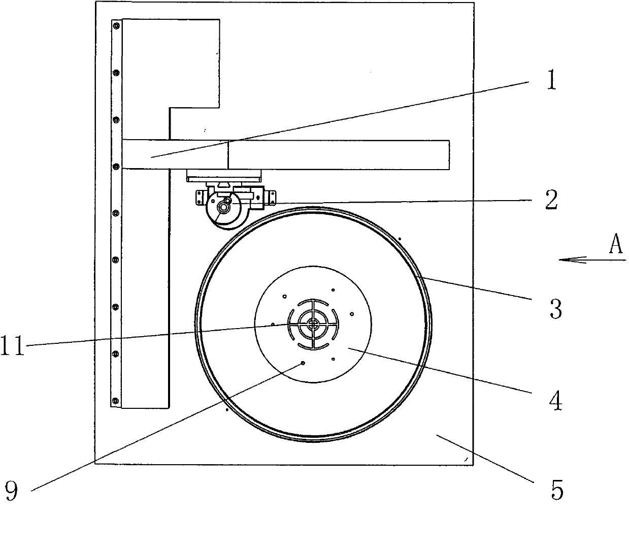
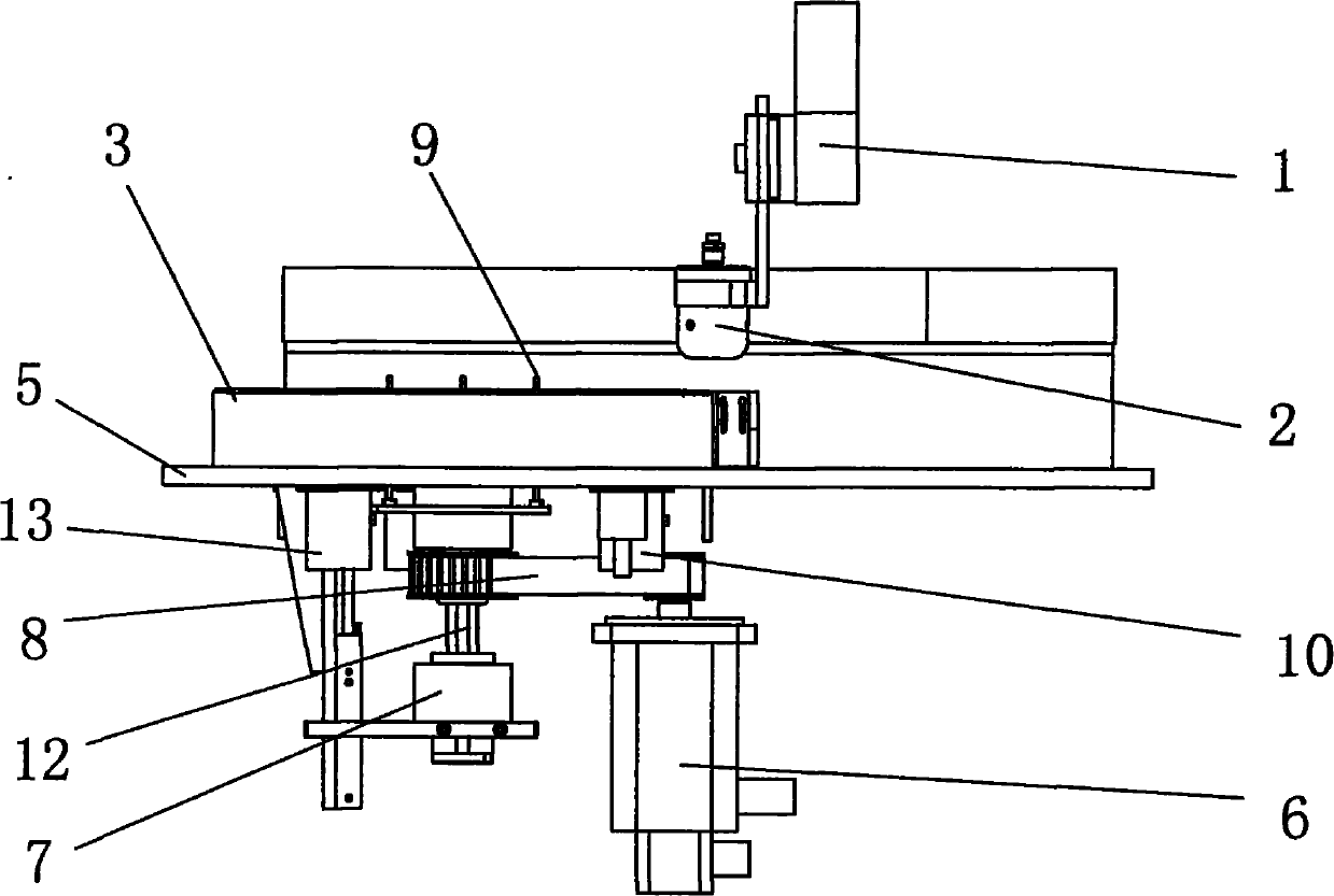
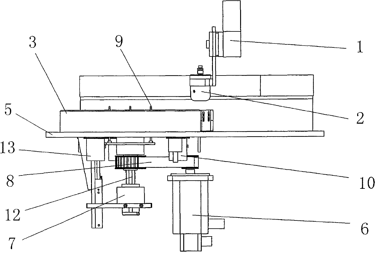
[0025] Such as Figure 1-2 As shown, the glue spray processing device of the present invention mainly includes: a linear actuator 1, a nozzle 2, a protective cup 3, a slide table 4, a unit base 5, a rotating motor 6, a conductive slip ring 7, a timing belt 8, and a bracket 9 , exhaust duct 10, vacuum chuck 11, etc., the unit base surface 5 is provided with a protective cup 3, a slide table 4, a vacuum chuck 11, and the slide table 4 and the vacuum chuck 11 are arranged on the inner side of the protective cup 3, and the slide The table 4 is used to place the wafer, and a vacuum chuck 11 is arranged on the bottom of the wafer, and the vacuum chuck 11 is located at the center of the loading table 4 . A linear actuator 1 is provided above the unit base surface 5 , and the nozzle 2 is installed on the linear actuator 1 . Below the unit base surface 5, a ro...


PUM


Abstract

The invention relates to a glue spraying processing technology in the micro electro mechanical system process, in particular to a glue spraying processing device used in the semiconductor manufacturing process, and the device formed by uniformly coating photoresist or a protection isolation layer on the wafer surface which is rough or is provided with deep holes, is applicable to three-dimensional packaging in the semiconductor field. A linear actuator is arranged above the unit base surface of the glue spraying processing device, the linear actuator is provided with a nozzle used for spraying glue onto a wafer, and the unit base surface is provided with a wafer carrying platform used for placing the wafer. The device is not only applicable to common photoinduced corrosion inhibitors but also applicable to photoinduced corrosion inhibitors with higher viscosity, the viscosity of the photoinduced corrosion inhibitor with higher viscosity can be reduced by diluting and blending, the photoinduced corrosion inhibitor is uniformly sprayed onto the wafer surface which is rough, and process requirements of the wafer to be processed are ensured.

Description

Technical field: [0001] The invention relates to the glue spraying treatment technology in the micro-electromechanical (mems) process, in particular to a glue spraying treatment device used in the semiconductor manufacturing process, which uniformly coats the surface of the wafer with rough surface or deep hole by photolithography A device for glue or protective isolation layers, suitable for three-dimensional (3d) packaging in the semiconductor field. Background technique: [0002] Part of the bump packaging process requires that a photoresist or a protective isolation layer be coated on the surface of the wafer with a highly undulating surface or a wafer with deep holes. This isolation layer requires uniform thickness at all points, whether it is at the corner of the slope. Consistent, while the traditional glue drop spin coating process can only fill up the undulations or deep holes to form a plane, because the coating thickness of each point is different, resulting in va...

Claims


Application Information

Patent Timeline
Patent Type & Authority Applications(China)
IPC IPC(8): B81C1/00B81C3/00B05B13/02B05B13/04B05B17/06B05C5/00B05C13/02
Inventor 汪明波
Owner SHENYANG KINGSEMI CO LTD
Why Eureka
Try Eureka