Method for preparing silicon-based SIS heterojunction photoelectric device

A photoelectric device, heterojunction technology, applied in the direction of electrical components, semiconductor devices, circuits, etc., can solve the problem of high cost

Inactive Publication Date: 2011-04-27
SHANGHAI UNIV
View PDF0 Cites 16 Cited by
  • Summary
  • Abstract
  • Description
  • Claims
  • Application Information

AI Technical Summary

Problems solved by technology

In the popularization and application of sola

Method used


Image

  • Method for preparing silicon-based SIS heterojunction photoelectric device
  • Method for preparing silicon-based SIS heterojunction photoelectric device
  • Method for preparing silicon-based SIS heterojunction photoelectric device

Examples


Embodiment 1

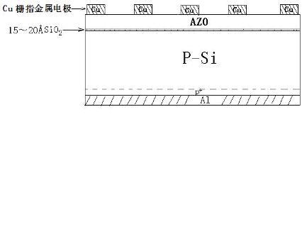
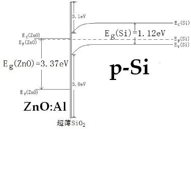
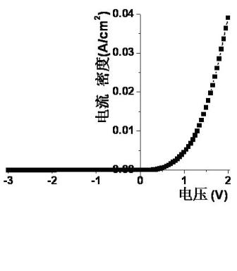
[0040] In this embodiment, the preparation method of the novel SINP silicon blue-violet light cell is as follows:

[0041](1) A p-type Czochralski silicon single wafer with a crystal orientation of (100), a resistivity of 5.0 Ω·cm, and a thickness of 200 μm was selected as the substrate.

[0042] (2) By the standard RCA cleaning technology, the silicon wafer is first cleaned at 75°C NH 4 OH:H 2 o 2 :H 2 O volume ratio of 1:1:5 mixed solution ultrasonic cleaning for 10 minutes. After rinsing with deionized water, HCl:H at 75°C 2 o 2 : H 2 O volume ratio is 1:1:6 mixed solution ultrasonic cleaning for 10 minutes.

[0043] (3) Dilute hydrochloric acid (volume ratio is HCl:H 2 O=1:6) cleaning, and then after cleaning with deionized water, use ordinary N 2 Air dry.

[0044] (4) Put the silicon wafer at a volume ratio of HF:H 2 Soak in O=1:10 solution for 7 minutes to remove the phosphosilicate glass on the front and the natural oxide layer on the silicon surface. ...


PUM

PropertyMeasurementUnit
Resistivityaaaaaaaaaa
Thicknessaaaaaaaaaa

Abstract

The invention relates to a method for preparing a direct current (DC) magnetron sputtering AZO/SiO2/p-SiSIS heterojunction photoelectric device, and belongs to the technical field of methods for preparing silicon-based heterojunction photoelectric devices. By growth of an ultrathin SiO2 layer through low-temperature thermal oxidation, DC magnetron sputtering of an AZO emitter, antireflection and collection of an electrode film, a novel AZO/SiO2/p-SiSIS ultraviolet-visible-near-infrared broad-spectrum heterojunction photoelectric device is successfully prepared. An I/V curve of the prepared AZO/SiO2/p-SiSIS heterojunction has good rectification characterisitic and very low reverse dark current, so a good heterojunction diode is formed between AZO and p-Si. Under the condition of AM 1.5 illumination, the open-circuit voltage VOC is 230mV, the photoelectric conversion efficiency eta is 0.025 percent, and the photovoltaic effect is obvious. By combining different characteristics of a wide band gap of the AZO and a relatively narrow band gap of a Si material for mutual complementation, the SIS heterojunction can be developed into a low-cost solar cell, and also can become an excellent-performance ultraviolet-visible-near-infrared enhanced broad-spectrum photoelectric detector.

Description

technical field [0001] The invention relates to a novel DC magnetron sputtering AZO / SiO 2 The invention relates to a preparation method of a p-Si SIS heterojunction photoelectric device, which belongs to the technical field of preparation methods of novel silicon-based heterojunction photoelectric devices. Background technique [0002] In recent years, from the perspective of preventing the global warming effect, protecting the environment and replacing petroleum energy, the use of solar power has received great attention. In the popularization and application of solar cells, the biggest obstacle is its high cost. Therefore, how to reduce the cost is one of the most important research topics at present. There are many ways to reduce the cost of solar cells, such as reducing the cost of silicon materials, improving existing technologies, adopting new technologies, and adopting cheap junction methods. [0003] SIS (abbreviation of Semiconductor / Insulator / Semiconductor str...

Claims


Application Information

Patent Timeline
IPC IPC(8): H01L31/18
CPCY02P70/50
Inventor 马忠权何波赵磊
Owner SHANGHAI UNIV
Why Eureka
Try Eureka