Hybrid latch applied to multi-power supply system on chip

A system-on-chip, hybrid technology, applied in electrical components, output power conversion devices, etc., can solve problems such as limiting the standby time of handheld devices, inverter short-circuit current, etc., to reduce battery consumption and suppress short-circuit current.

Active Publication Date: 2013-07-24
SHANGHAI HUAHONG GRACE SEMICON MFG CORP
View PDF3 Cites 0 Cited by
  • Summary
  • Abstract
  • Description
  • Claims
  • Application Information

AI Technical Summary

Problems solved by technology

[0007] like figure 2 As shown, a major problem of the existing multi-power system-on-chip power-on short-circuit current suppression circuit is that when VDD1.8 reaches 1.8V and stabilizes, the first-stage inverter itself has a short-circuit current, because the inverter must Provided by a 5V power supply, when the input terminal is 1.8V, although the voltage at the flip point is adjusted to make it output a correct logic value, but because the NMOS transistor in the inverter is turned on, the PMOS transistor cannot be turned off (the source-gate voltage of the PMOS transistor The value is 5V-1.8V=3.2V), so the inverter will have a short-circuit current of tens of microamps to hundreds of microamps
The short-circuit current will always exist after the power-on is completed and stabilized, and the handheld device is usually in the standby / working state for several hours or consecutive days after it is turned on. The short-circuit current of tens of microamps that lasts for such a long time is also a big meaningless problem. consumption, which ultimately limits the standby time of the handheld

Method used


Image

  • Hybrid latch applied to multi-power supply system on chip
  • Hybrid latch applied to multi-power supply system on chip
  • Hybrid latch applied to multi-power supply system on chip

Examples


Embodiment Construction

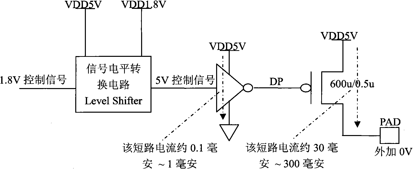
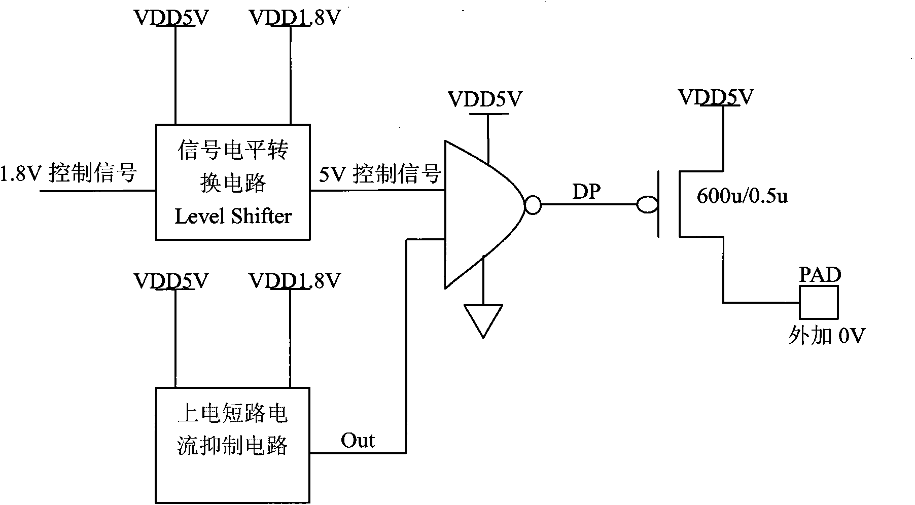
[0023] Such as Figure 4 As shown, it is a hybrid latch applied to a system-on-chip with multiple power supplies according to the present invention. The multi-power supply system-on-a-chip refers to a system in which the main power supply and multiple sub-power supplies are integrated on one working chip for collaborative power supply. The working chip includes multiple working circuits, and some working circuits will generate short-circuit current when the sub-power supplies are not stable. In this embodiment, the total power supply is a 5V power supply, and the sub-power supply is a 1.8V power supply, and the sub-power supplies are generated by a power generation circuit using the total power supply as a source. The input terminal of the hybrid latch is connected to the main power supply and the sub-power supply, and the output terminal is connected to the part of the working circuit of the working chip that will generate a short-circuit current when the sub-power supply is ...


PUM


Abstract

The invention discloses a hybrid latch applied to a multi-power supply system on chip. The multi-power supply system on chip is a system in which a main power supply and a plurality of branch power supplies are integrated on a working chip for synergetic power supply, and a working chip comprises a plurality of working circuits. The hybrid latch comprises a two-input nor gate, a two-input nand gate, a pull-up P-channel metal oxide semiconductor (PMOS) transistor, a pull-down N-channel metal oxide semiconductor (NMOS) transistor and a phase inverter, wherein the input end and the output end ofthe nor gate are connected with the input end and the output end of the nand gate; the other input end of the nor gate is connected with the main power supply; the other end of the nand gate is connected with the branch power supplies; the pull-up PMOS transistor and the pull-down NMOS transistor are connected with the output ends of the nor gate and the nand gate respectively; and the output endof the nor gate is connected with the phase inverter, so that a signal is output to a part of working circuits. When the branch power supplies are instable after the main power supply is electrified and becomes stable quickly, a connected working circuit can be switched off and short-circuit current of the working circuit disappears, so that the battery consumption of the multi-power supply system on chip can be lowered.

Description

technical field [0001] The invention relates to a hybrid latch applied to a multi-power supply system on chip. Background technique [0002] With the increasing complexity of the current System on a chip (SoC), it is very common to use multiple groups of power supplies with different voltages on a single chip. A typical example is a chip designed on a 0.18-micron process, its internal voltage is generally 1.8V, and the input and output circuit (IO) part uses 5V or 3.3V (5V is used for discussion in this article). communicate externally. figure 1 Shown is a schematic diagram of the input and output circuits of the existing multi-power system on chip, the circuit includes a 5V power supply VDD5V and a 1.8V power supply VDD1.8V, a signal level shifter (Level Shifter), an inverter and a PMOS transistor; here The 5V power supply corresponds to the IO external circuit power supply of the SoC, and the 1.8V power supply corresponds to the working power supply of the internal circu...

Claims


Application Information

Patent Timeline
Patent Type & Authority Patents(China)
IPC IPC(8): H02M1/32
Inventor 杨俊
Owner SHANGHAI HUAHONG GRACE SEMICON MFG CORP
Why Eureka
Try Eureka