Semiconductor chip assembly with post/base heat spreader and conductive trace

A technology for semiconductors and chipsets, applied in semiconductor devices, semiconductor/solid-state device components, and electrical solid-state devices, etc., and can solve the problems of limited routing capability, excessive volume, and unsuitable for low-cost mass production operations.

Inactive Publication Date: 2011-05-25
BRIDGE SEMICON
View PDF9 Cites 11 Cited by
  • Summary
  • Abstract
  • Description
  • Claims
  • Application Information

AI Technical Summary

Problems solved by technology

If the substrate is a single-layer circuit system, the routing capability is limited, but if the substrate is a multi-layer circuit system, its excessively thick dielectric layer will reduce the heat dissipation effect
In addition, the technology of the aforementioned case sti...

Method used


Image

  • Semiconductor chip assembly with post/base heat spreader and conductive trace
  • Semiconductor chip assembly with post/base heat spreader and conductive trace
  • Semiconductor chip assembly with post/base heat spreader and conductive trace

Examples


Embodiment Construction

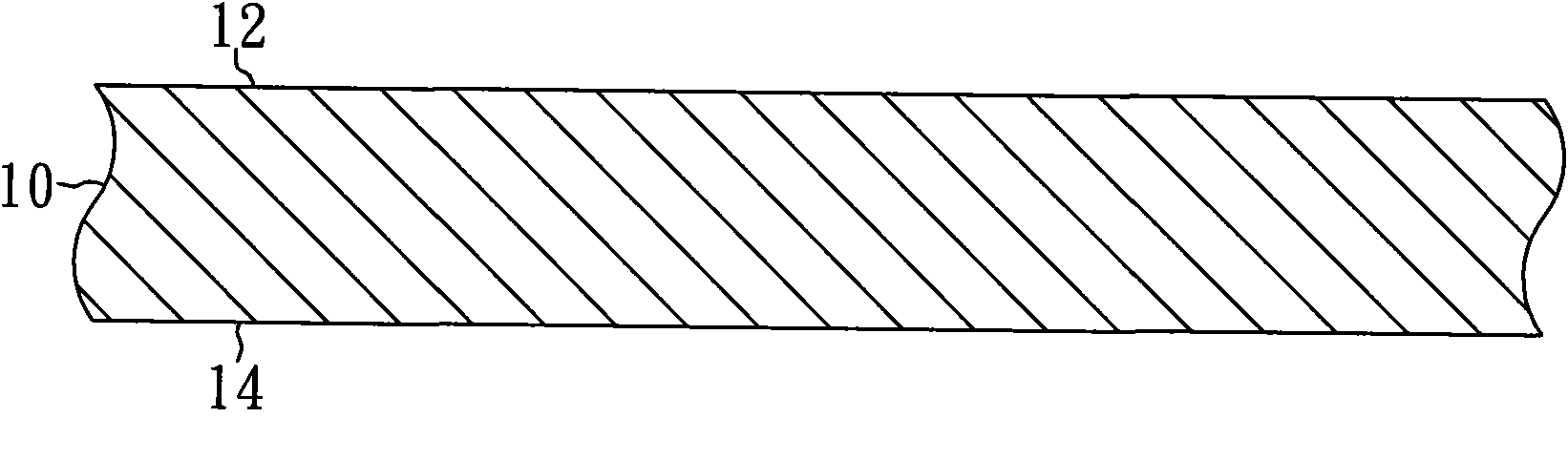
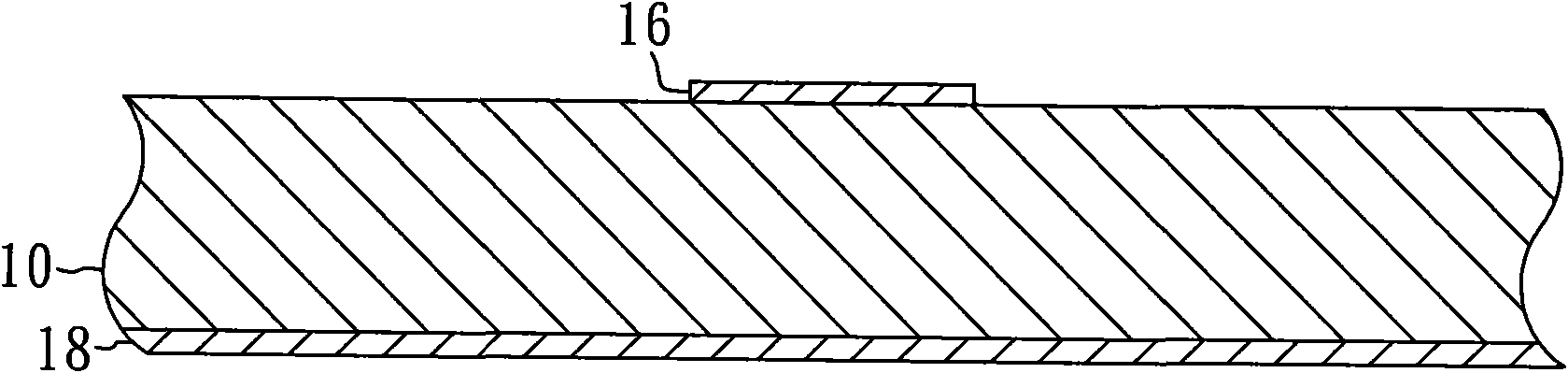
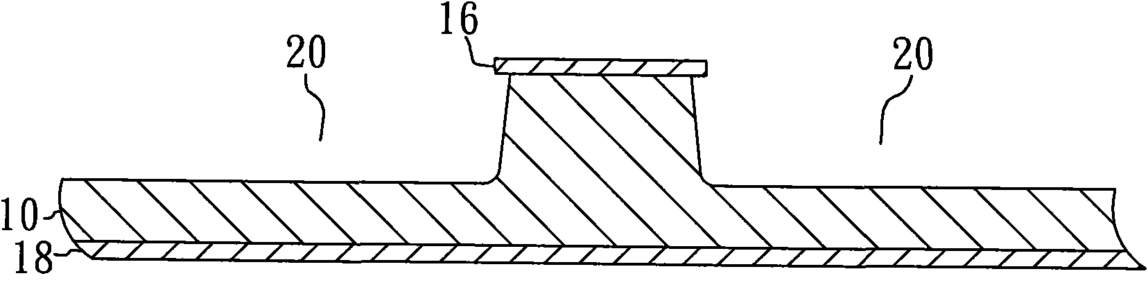
[0074] Figure 1 to Figure 4 It is a cross-sectional view illustrating a method for manufacturing a post and a base in an embodiment of the present invention, Figure 5 and Image 6 respectively Figure 4 top and bottom views.

[0075] figure 1 Is a cross-sectional view of a metal plate 10 comprising opposing major surfaces 12 and 14 . The illustrated metal plate 10 is a copper plate having a thickness of 500 microns. Copper has the advantages of high thermal conductivity, good bonding and low cost. The metal plate 10 can be made of various metals such as copper, aluminum, iron-nickel alloy, iron, nickel, silver, gold, mixtures thereof and alloys thereof.

[0076] figure 2 It is a cross-sectional view showing a patterned etch stop layer 16 and a fully covered etch stop layer 18 formed on the metal plate 10 . The patterned etch resist layer 16 and the fully covered etch resist layer 18 shown in the figure are photoresist layers deposited on the metal plate 10, which are ...


PUM


Abstract

A semiconductor chip assembly includes a semiconductor device, a heat spreader, a conductive trace and an adhesive. The semiconductor device is electrically connected to the conductive trace and thermally connected to the heat spreader. The heat spreader includes a post and a base. The post extends upwardly from the base into an opening in the adhesive, and the base extends laterally from the post. The adhesive extends between the post and the conductive trace and between the base and the conductive trace. The conductive trace provides signal routing between a pad and a terminal.

Description

technical field [0001] The invention relates to a semiconductor chip group body, in particular to a semiconductor chip group body composed of semiconductor elements, wires, adhesive layers and heat sinks and a manufacturing method thereof. Background technique [0002] Semiconductor components such as packaged and unpackaged semiconductor chips can provide high voltage, high frequency and high performance applications; these applications require high power consumption to perform specific functions, but the higher the power, the semiconductor components generate heat more and more. In addition, after the packaging density is increased and the size is reduced, the surface area available for heat dissipation is reduced, resulting in increased heat generation. [0003] Semiconductor components are prone to problems such as performance degradation and shortened service life under high temperature operation, and may even fail immediately. High heat not only affects chip performa...

Claims


Application Information

Patent Timeline
Owner BRIDGE SEMICON
Why Eureka
Try Eureka