Method of manufacturing organic el display unit and organic el display unit

A display unit, an organic technology, applied in semiconductor/solid-state device manufacturing, electrical components, devices for coating liquid on the surface, etc., can solve high equipment manufacturing costs, difficult separation and coating of metal masks, and large screens that cannot be applied Substrate and other issues to achieve the effect of improving luminous efficiency and life, and improving the interface state

Active Publication Date: 2011-06-01
JOLED INC
View PDF6 Cites 19 Cited by
  • Summary
  • Abstract
  • Description
  • Claims
  • Application Information

AI Technical Summary

Problems solved by technology

That is, in particular, it is difficult to perform separate coating by using a metal mask
Specifically, when forming large panels, the vacuum evaporation method leads to high equipment manufacturing costs, which cannot be applied to large-screen substrates, and is not suitable for mass production

Method used


Image

  • Method of manufacturing organic el display unit and organic el display unit
  • Method of manufacturing organic el display unit and organic el display unit
  • Method of manufacturing organic el display unit and organic el display unit

Examples


example 1

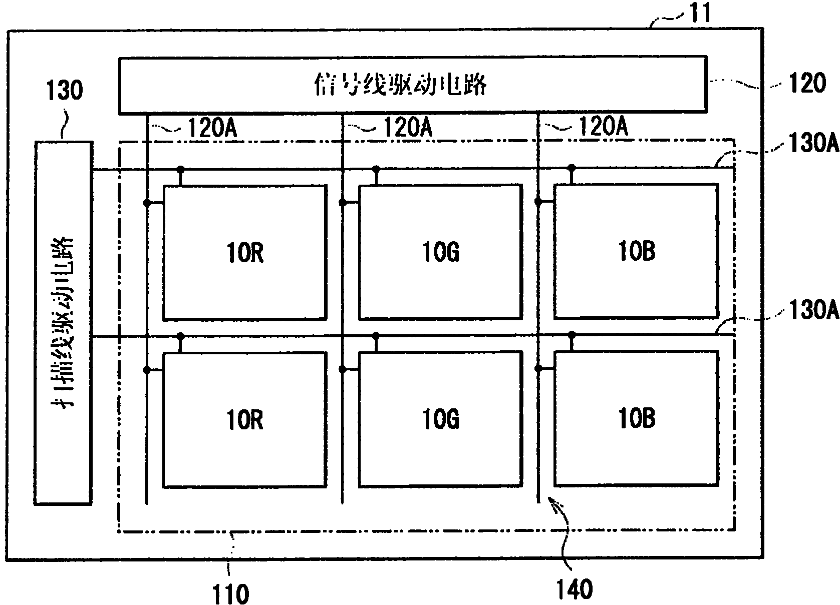
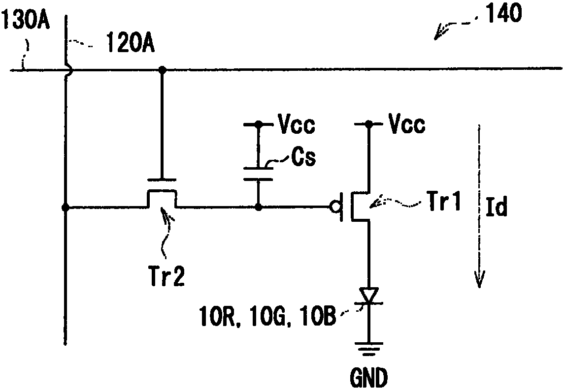
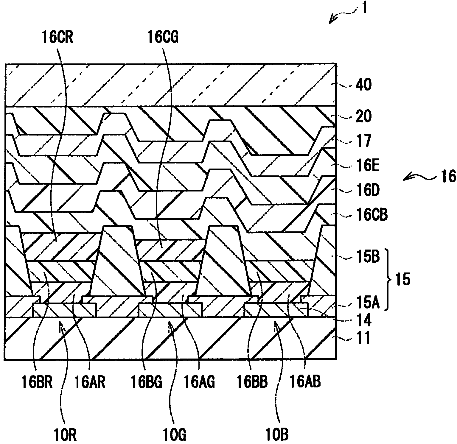
[0163] The substrates 11 were formed to have a size of 25 mm×25 mm for the red organic EL device 10R, the green organic EL device 10G, and the blue organic EL device 10B, respectively.

[0164] First, a glass substrate (25 mm×25 mm) was prepared as the substrate 11 . On the substrate 11, a two-layer structure consisting of a silver alloy layer made of Ag-Pd-Cu alloy with a thickness of 120 nm and a transparent conductive film made of ITO with a thickness of 10 nm was formed as the lower electrode 14 (step S101).

[0165]Subsequently, as the hole injection layers 16AR, 16AG, and 16AB, ND 1501 (polyaniline, manufactured by Nissan Chemical Industries Ltd) was coated in air by a spin coating method to have a thickness of 15 nm, and was applied on a hot plate at 220 degrees Celsius. The resulting product is thermally cured for 30 minutes (step S104).

[0166] Thereafter, at N 2 (dew point: -60 degrees Celsius, oxygen concentration: 10 ppm) as a hole transport layer by coating the...

example 2

[0195] An organic EL display unit was fabricated in the same manner as in Example 1, except that in the step of forming the hole transport layer 16BB of the blue organic EL device 10B described in Example 1, the structural formula 1 (58 ).

[0196] Chemical formula 16

[0197] Compound 1(58)

[0198]

example 3

[0200] An organic EL display unit was fabricated in the same manner as in Example 1, except that in the step of forming the hole transport layer 16BB of the blue organic EL device 10B described in Example 1, the structural formula 1 (22 ).

[0201] Chemical formula 17

[0202] Structural formula 1(22)

[0203]


PUM

PropertyMeasurementUnit
thicknessaaaaaaaaaa
thicknessaaaaaaaaaa
thicknessaaaaaaaaaa

Abstract

A method of manufacturing an organic EL display unit and an organic EL display unit capable of improving light emitting efficiency and life of blue are provided. A hole injection layer are formed on a lower electrode. For a red organic EL device and a green organic EL device, a hole transport layer, a red light emitting layer, and a green light emitting layer made of a polymer material are formed. A hole transport layer made of a low molecular material is formed on the hole injection layer of a blue organic EL device. A blue light emitting layer made of a low molecular material is formed on the red light emitting layer, the green light emitting layer, and the hole transport layer for the blue organic EL device. An electron transport layer, an electron injection layer, and an upper electrode are sequentially formed on the blue light emitting layer.

Description

technical field [0001] The present invention relates to a method of manufacturing an organic EL display unit that emits light by using an organic electroluminescence (EL) phenomenon, and an organic EL display unit. Background technique [0002] With the accelerated development of the information communication industry, a display device with high performance is required. In particular, organic EL devices have been attracting attention as next-generation display devices. As a self-luminous display device, an organic EL device has the advantages of wide viewing angle and good contrast. In addition, organic EL devices have an advantage of short response time. [0003] A light emitting layer and the like forming an organic EL device are roughly classified into low-molecular materials and polymer materials. In general, it is known that low-molecular materials provide higher luminous efficiency and have longer lifetime. In particular, low-molecular materials provide higher perf...

Claims


Application Information

Patent Timeline
Patent Type & Authority Applications(China)
IPC IPC(8): H01L51/56B05D1/02B05D7/00H01L51/50H01L51/54H01L27/32
CPCH01L51/56H01L51/0026H01L51/5048H01L51/0043H01L27/3211H01L51/0042H01L51/5012H01L51/0059H01L51/0058H01L51/0081H01L51/0003H10K59/35H10K71/12H10K71/40H10K85/146H10K85/151H10K85/626H10K85/631H10K85/324H10K50/14H10K50/11H10K71/00
Inventor 尾花良哲肥后智之
Owner JOLED INC
Why Eureka
Try Eureka