Thick-film photoresist cleaning solution and cleaning method thereof

A technology of cleaning solution and photoresist, which is applied in the processing of photosensitive materials, etc., can solve the problems of insufficient cleaning ability, strong corrosion of semiconductor wafer patterns and substrates, etc., and achieve the effect of inhibiting corrosion

Inactive Publication Date: 2011-06-15
ANJI MICROELECTRONICS (SHANGHAI) CO LTD
View PDF7 Cites 4 Cited by
  • Summary
  • Abstract
  • Description
  • Claims
  • Application Information

AI Technical Summary

Problems solved by technology

[0009] The technical problem to be solved by the present invention is to provide a method for cleaning thick-film photoresist in view of the insufficient cleaning ability of existing thick-film photoresist

Method used


Image

  • Thick-film photoresist cleaning solution and cleaning method thereof
  • Thick-film photoresist cleaning solution and cleaning method thereof
  • Thick-film photoresist cleaning solution and cleaning method thereof

Examples


Embodiment Construction

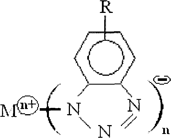
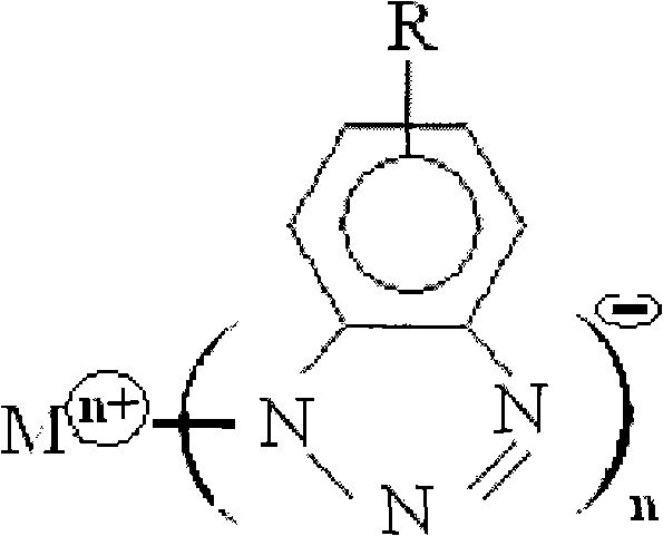
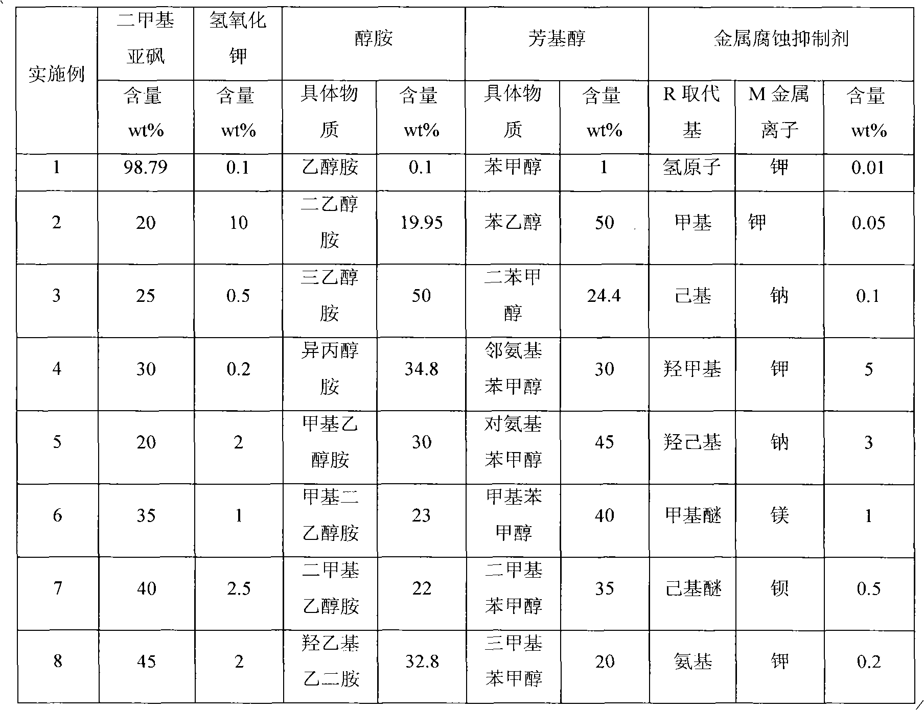
[0022] The present invention will be further described below through specific embodiments. The cleaning solution of the present invention can be obtained by uniformly mixing according to the distribution ratio of the components in the table.

[0023] Component and content of cleaning agent in table 1 embodiment 1~25

[0024]

[0025]

[0026] Table 2 part embodiment and comparative example formula

[0027]

[0028] Note: NA means that this component was not added.

[0029] In order to further illustrate the effect and principle of the present invention, the solutions in Table 2 are specially configured, see Table 2 for details. It should be noted that comparative example 1' cannot form a uniform solution in Table 2, which shows that the solubility of KOH in dimethyl sulfoxide is less. Comparative Example 2' shows that adding aryl alcohol, i.e. benzyl alcohol, can improve the solubility of KOH in the system and form a uniform solution. In order to further investiga...


PUM


Abstract

The invention discloses thick-film photoresist cleaning solution and a cleaning method thereof. The photoresist cleaning solution comprises dimethyl sulfoxide, potassium hydroxide, aryl alcohol, alcohol amine and a metal corrosion inhibitor. The photoresist cleaning solution can be used in a wider temperature range from 30 to 90 DEG C, is used for removing thicker photoresist on a metal, a metal alloy or a dielectric medium and other substrates in a semiconductor manufacturing process, and is particularly suitable for removing high-crosslinking degree negative photoresist with the thickness of over 100 mu m. Meanwhile, the photoresist cleaning solution has extremely weak corrosion on copper, tin, lead and other metals, does not damage chip patterns and substrates, and has good application prospect in the fields of microelectronics, such as semiconductor chip cleaning and the like.

Description

technical field [0001] The invention relates to a low-etching thick-film photoresist cleaning solution and a cleaning method thereof. Background technique [0002] In the usual semiconductor manufacturing process, a photoresist mask is formed on the surface of metals such as silicon dioxide, Cu (copper), and low-k materials, and pattern transfer is performed by wet or dry etching after exposure. In the wafer microsphere implantation process (bumping technology), a photoresist material (photoresist) is also required to form a mask, which also needs to be removed after the microspheres are successfully implanted, but due to the thicker photoresist , is often difficult to remove completely. The more common methods to improve the removal effect are to extend the soaking time, increase the soaking temperature and use more aggressive solutions, but this often causes corrosion of the wafer substrate and microspheres, resulting in a significant decrease in wafer yield. [0003] At...

Claims


Application Information

Patent Timeline
IPC IPC(8): G03F7/42
Inventor 刘兵彭洪修孙广胜
Owner ANJI MICROELECTRONICS (SHANGHAI) CO LTD
Why Eureka
Try Eureka