CMOS (Complementary Metal-Oxide-Semiconductor) transistor and stress memory treatment method thereof

A technology of stress memory and processing method, which is applied in the direction of transistor, semiconductor/solid-state device manufacturing, electrical components, etc., can solve the problems of not adapting to the development trend of integrated circuit miniaturization, unsatisfactory effect, product stability and yield impact, etc. Achieve the effects of improving stability and yield, saving costs, and reducing the probability of occurrence

Active Publication Date: 2011-06-15
SEMICON MFG INT (SHANGHAI) CORP +1
View PDF1 Cites 20 Cited by
  • Summary
  • Abstract
  • Description
  • Claims
  • Application Information

AI Technical Summary

Problems solved by technology

However, CMOS transistors processed by SMT are more likely and more likely to be affected by PID, resulting in affected product stability and yield
[0006] In the United States Invention Patent Application Publication No. US20090224326A1 published on September 10, 2009, a method of using a protection circuit to reduce PID is disclosed, but obviously, adding a protection circuit will increase the area of ​​the entire integrated circuit, which is not suitable for Development Trend of IC Miniaturization
There are also some other attempts to reduce the PID phenomenon after the SMT process in the prior art, such as reducing the deposition temperature of the stress silicon nitride layer in the SMT, and converting the process of depositing the buffer oxide layer from LDSRO (Low Deposition Rate Silicon Rich Oxide, low Speed ​​deposition of silicon-rich oxide) to SACVD (Sub-Atmospheric Chemical Vapor Deposition, sub-atmospheric chemical vapor deposition), or change the etching bias of the stressed silicon nitride layer, etc., but a large number of experimental results show that the effects of the above methods are not Not ideal, the probability of PID in CMOS transistors after SMT is still high

Method used


Image

  • CMOS (Complementary Metal-Oxide-Semiconductor) transistor and stress memory treatment method thereof
  • CMOS (Complementary Metal-Oxide-Semiconductor) transistor and stress memory treatment method thereof
  • CMOS (Complementary Metal-Oxide-Semiconductor) transistor and stress memory treatment method thereof

Examples


Embodiment 1

[0037] This embodiment provides a stress memory processing method for CMOS transistors, such as Figure 7 shown, including:

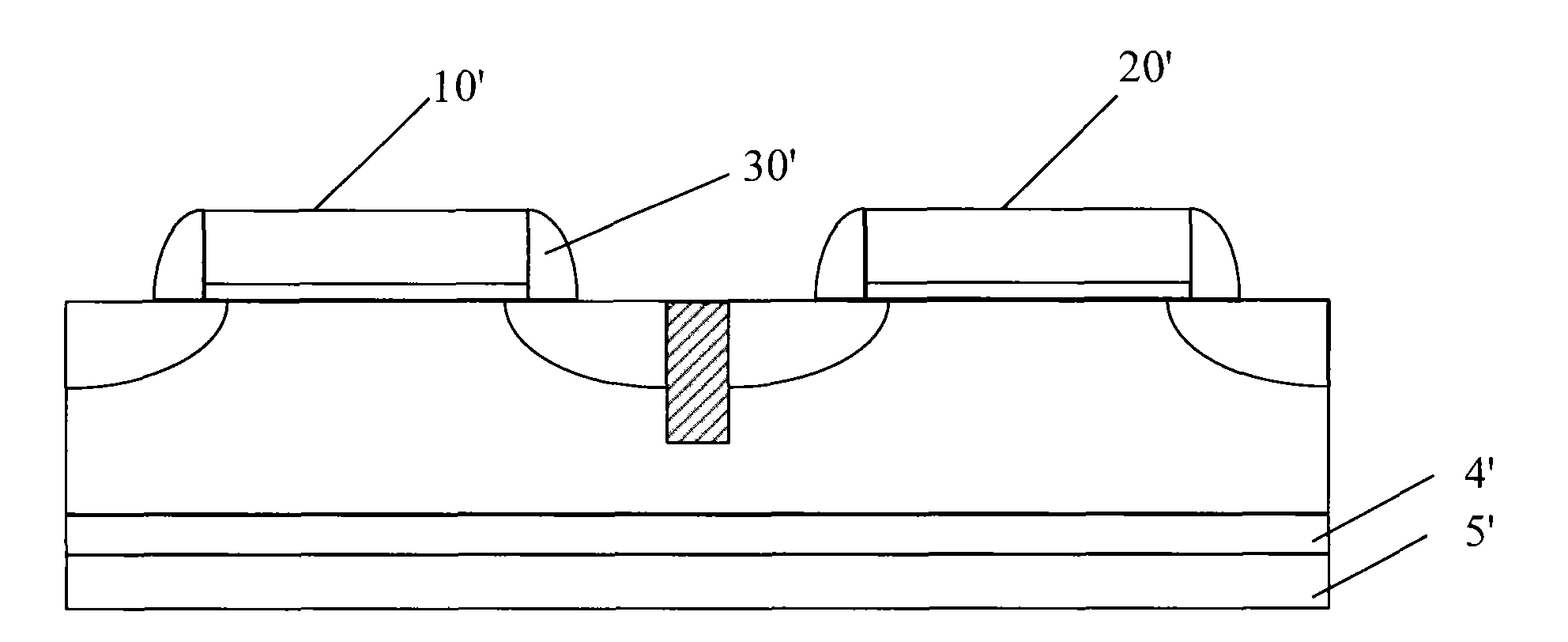
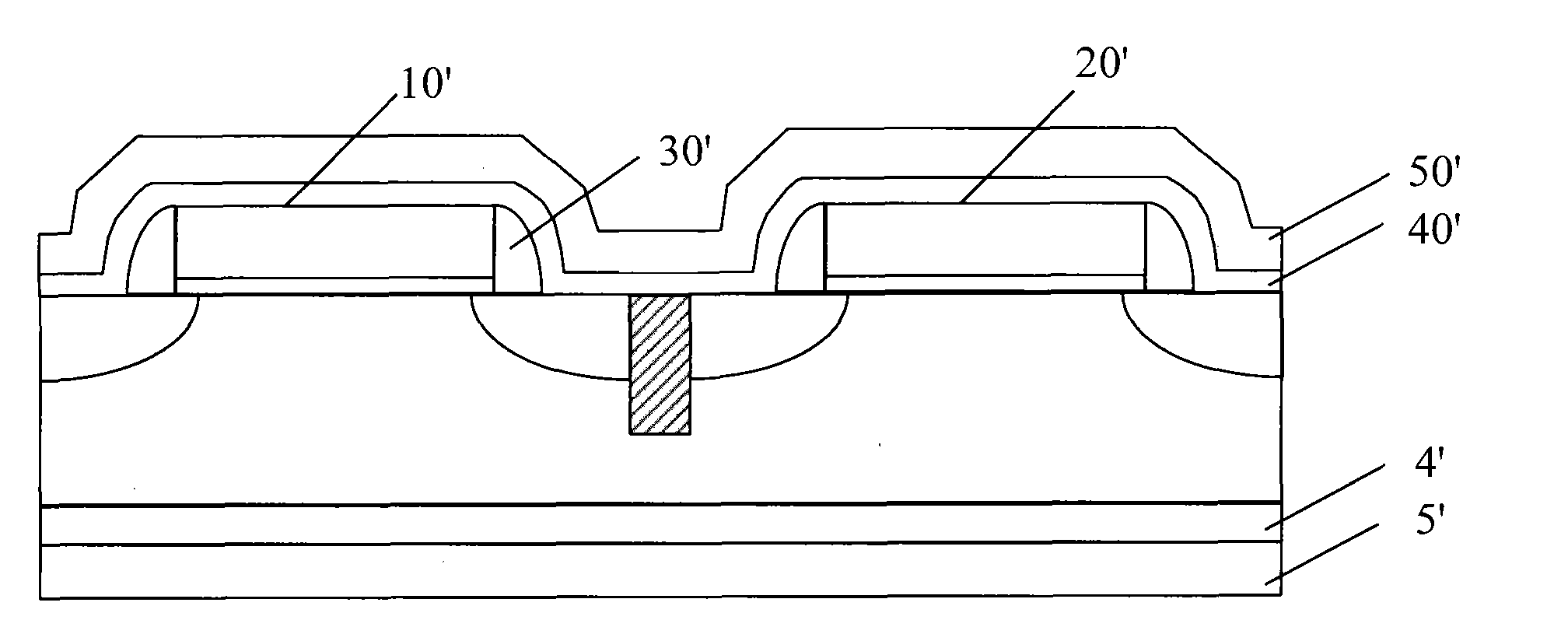
[0038] S101, providing a substrate formed with CMOS transistors.

[0039] Each CMOS transistor includes a gate, a source, a drain, a conductive channel, a gate oxide layer and a gate sidewall, the inner layer of the gate sidewall is a silicon oxide layer, and the outer layer is a silicon nitride layer. Wherein, the source, the drain and the conductive channel are located in the well of the reverse type of the source / drain in the substrate (the technical solution of the present invention is not involved, and are simplified and not shown in the accompanying drawings) and are located in the source Between the electrode and the drain, the gate oxide layer is located on the upper surface of the substrate corresponding to the position of the conductive channel, the gate (usually polysilicon) is located on the upper surface of the gate oxide layer, and the si...

Embodiment 2

[0073] The present invention also provides a CMOS transistor, such as Figure 21 shown.

[0074] The CMOS transistor includes a gate, a source, a drain, a conductive channel (not shown in the figure), a gate oxide layer 22 and a gate sidewall 33, and the inner layer of the gate sidewall 33 is a silicon oxide layer , the outer layer is a silicon nitride layer, and the lower surface of the substrate 11 where the CMOS transistor is located has a silicon oxide layer 44 and a silicon nitride layer 55 corresponding to the gate sidewall 33;

[0075] Among the CMOS transistors, the conduction channel of the NMOS transistor 66 has compressive stress, and the conduction channel of the PMOS transistor 77 has no stress.

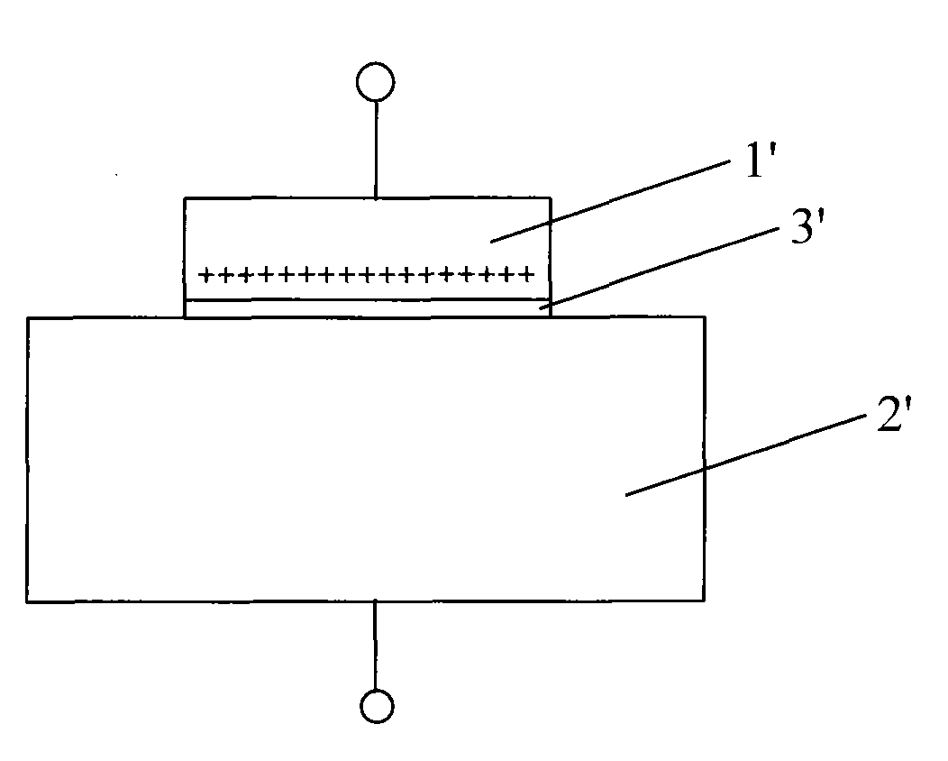
[0076] The CMOS transistor of the present invention increases the thickness T of the insulating layer by retaining the silicon oxide layer and the silicon nitride layer on the lower surface of the substrate, thereby reducing the electric field E formed on the substrate ...


PUM


Abstract

The invention discloses a CMOS (Complementary Metal-Oxide-Semiconductor) transistor and a stress memory treatment method thereof. The method comprises the following steps of: providing a substrate with a formed CMOS transistor, wherein the lower surface of the substrate is provided with a silicon oxide layer corresponding to the inner layer of the side wall of a grid of the CMOS transistor and a silicon nitride layer corresponding to the outer layer of the side wall of the grid; sequentially depositing a buffer oxide layer and a stress silicon nitride layer on the upper surface of the CMOS transistor; removing the stress silicon nitride layer on the upper surface of a PMOS (P-channel Metal Oxide Semiconductor) transistor and annealing the substrate if the CMOS transistor comprises a NMOS (N-channel Metal Oxide Semiconductor) transistor and the PMOS transistor; directly annealing the substrate if the CMOS transistor comprises the NMOS transistor; and removing the stress silicon nitride layer on the upper surface of the NMOS transistor and the buffer oxide layer and keeping the silicon oxide layer and the silicon nitride layer, corresponding to the side wall of the grid, on the lower surface of the substrate. The stress memory treatment method in the invention is favorable for decreasing the occurrence probability of PID (Proportion Integration Differentiation) and saving cost, and is simple.

Description

technical field [0001] The invention relates to the technical field of semiconductor device manufacturing, in particular to a stress memory processing method for a CMOS transistor and the CMOS transistor. Background technique [0002] Plasma processing has been widely used in the field of semiconductor device manufacturing. However, during the manufacturing process, the plasma will accumulate on the gate 1' of the device (see figure 1 ), when the accumulated plasma charge reaches a certain threshold amount, the electric field on the gate oxide layer 3' between the gate 1' and the substrate 2' will break down the gate oxide layer 3' and damage the device, this The phenomenon is called PID (Plasma Induced Damage, plasma induced damage). [0003] PID is more serious in the 65G (Generic) process than in the 65LL (Low Leakage) process, mainly because the 65G process requires more plasma treatment processes, such as the SMT (Stress Memorization Technology, stress memory technol...

Claims


Application Information

Patent Timeline
Patent Type & Authority Applications(China)
IPC IPC(8): H01L21/8238H01L27/092
Inventor 刘金华
Owner SEMICON MFG INT (SHANGHAI) CORP
Why Eureka
Try Eureka