Micron sensing element, and preparation method and application thereof

A technology of sensing elements and matrix materials, applied in optical elements, microstructure technology, microstructure devices, etc., can solve the problems of late health monitoring research, achieve simple and easy preparation methods, improve monitoring accuracy, and reduce energy consumption Effect

Inactive Publication Date: 2013-11-13
INST OF METAL RESEARCH - CHINESE ACAD OF SCI +1
View PDF0 Cites 0 Cited by
  • Summary
  • Abstract
  • Description
  • Claims
  • Application Information

AI Technical Summary

Problems solved by technology

In aerospace, research on health monitoring is late

Method used


Image

  • Micron sensing element, and preparation method and application thereof
  • Micron sensing element, and preparation method and application thereof
  • Micron sensing element, and preparation method and application thereof

Examples


Embodiment 1

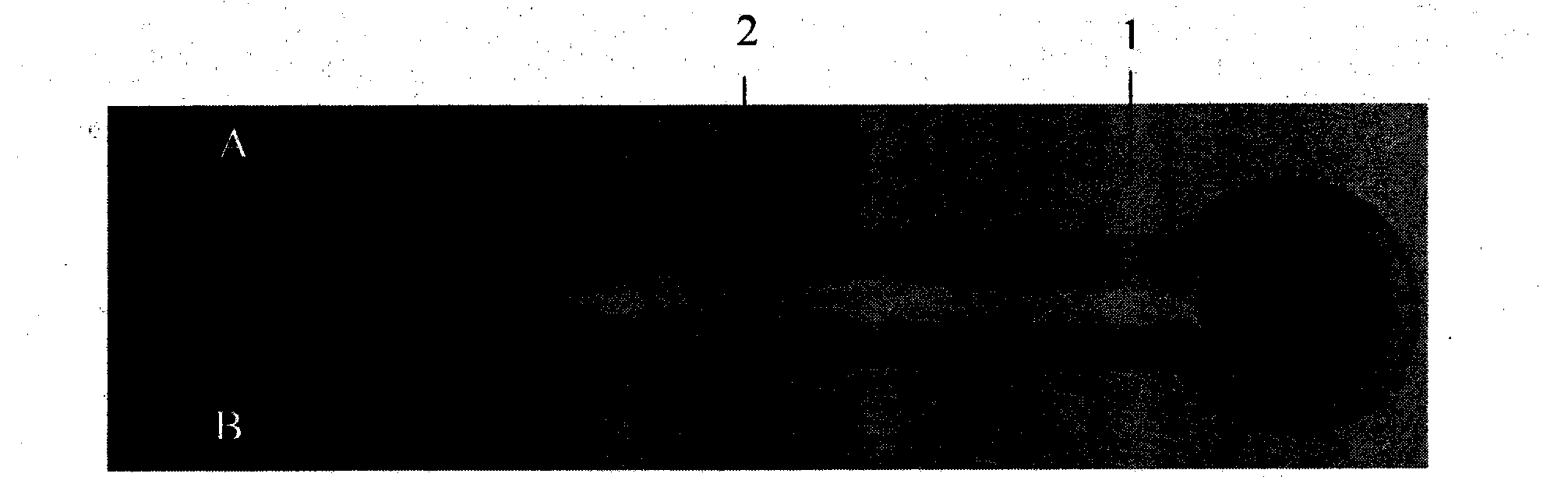
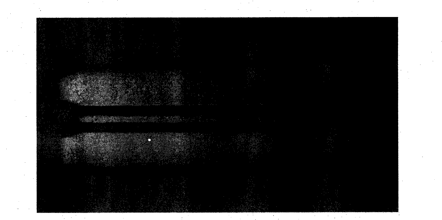
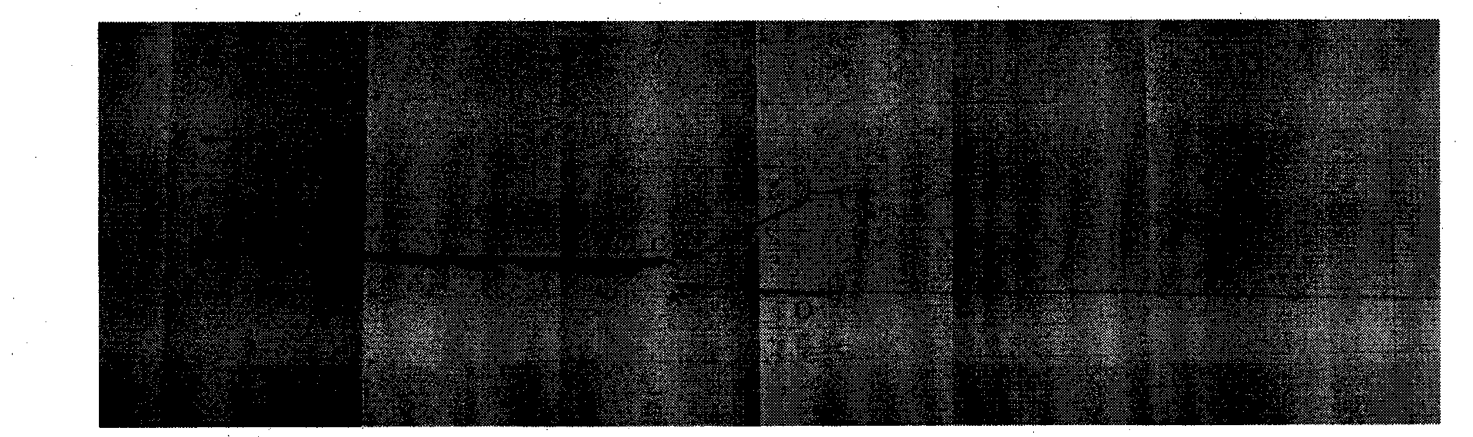
[0032] The surface of pure aluminum or aluminum alloy after anodic oxidation treatment is degreased, the sensor element template is adapted and fixed to the base material after anodic oxidation treatment, ultrasonically cleaned in trichlorethylene organic solvent for 5 minutes, and then installed on the card Put it into the vacuum chamber of the ion coating equipment, after vacuuming to 0.005Pa, pass the working gas argon into the vacuum chamber to a pressure of about 2Pa, apply a negative bias voltage of about 600 volts to the workpiece, and perform ion bombardment cleaning for 10 minutes; The evaporation source beam current is 50A, the workpiece is negatively biased at about 40 volts, and the copper film is deposited for 120 minutes, thus depositing a micron sensor element. The micron sensing element is composed of an insulating layer on the surface of the substrate 1 and a copper conductive film 2 deposited on the insulating layer. The thickness of the micron sensing element...

Embodiment 2

[0039] The difference from Example 1 is:

[0040] The surface of pure aluminum or aluminum alloy after anodic oxidation treatment is degreased, the sensor element template is adapted and fixed with the anodized base material, ultrasonically cleaned in trichlorethylene organic solvent for 10 minutes, and then installed on the card Put it on the tool and put it into the vacuum chamber of the ion coating equipment. After evacuating to 0.013Pa, pass the working gas argon into the vacuum chamber to a pressure of about 5Pa, apply a negative bias voltage of about 500 volts to the workpiece, and perform ion bombardment cleaning for 8 minutes; evaporate The source beam current is 80A, the workpiece is negatively biased at about 80 volts, and the copper film is deposited for 80 minutes, thereby depositing a micron sensing element. In this embodiment, the thickness of the micrometer sensing element is about 20 micrometers, and the width is about 10 millimeters.

[0041] In this embodime...

Embodiment 3

[0043] The difference from Example 1 is:

[0044] Remove oil stains on the surface of pure aluminum or aluminum alloy after anodic oxidation treatment, adapt and fix the sensor element template with the anodized substrate material, ultrasonically clean it in trichlorethylene organic solvent for 8 minutes, and then install the card on the card Put it on the tool and put it into the vacuum chamber of the ion coating equipment. After evacuating to 0.008Pa, pass the working gas argon into the vacuum chamber to a pressure of about 3Pa, apply a negative bias voltage of about 400 volts to the workpiece, and perform ion bombardment cleaning for 8 minutes; evaporate The source beam is 60A, the workpiece is negatively biased at about 60 volts, and the copper film is deposited for 40 minutes, thereby depositing a micron sensing element. In this embodiment, the thickness of the micrometer sensing element is about 8 micrometers, and the width is about 2 millimeters.

[0045] In this embod...


PUM

PropertyMeasurementUnit
thicknessaaaaaaaaaa
widthaaaaaaaaaa
thicknessaaaaaaaaaa

Abstract

The invention relates to a preparation technique technology of micron sensing elements, in particular to a micron sensing element which is highly integrated with a structural substrate and used for monitoring surface crack of a metal structure in real time, and preparation method and application thereof, for improving the reliability and monitoring accuracy of the sensing element, excluding error alarming condition, or, monitoring the health of air plane in real time, and monitoring the health of the classic metal structure such as aerospacecraft, large combination ship, warship, rapid train, large mechanical equipment, large bright, large power generator unit, nuclear power generation station and the like. In the invention, the micron sensing element highly integrated with the substrate material in the thickness of a plurality of microns and width of several millimeters is prepared on the substrate material surface by an ion plating technology. The preparation method comprises the following steps: insulating the substrate material surface, and controlling the shape of the micron sensing element with a template, then plating an electric conducting film on the surface of the insulating layer; and when the electric conducting film reaches the needed thickness, the micron sensing element is prepared.

Description

Technical field: [0001] The present invention relates to the manufacturing technology of micron sensing element, specifically a micron sensing element which is used for real-time monitoring of cracks on the surface of metal structure and is highly integrated with the structure matrix and its preparation method and application, which can be applied to the real-time health monitoring of aircraft. Monitoring can also be applied to the health monitoring of typical metal structures such as aerospace vehicles, large passenger and cargo ships, warships, express trains, large mechanical equipment, large bridges, large generator sets, and nuclear power plants. Background technique: [0002] In 1979, the US National Aeronautics and Space Administration (NASA) started a Fiber Optic Smart Structures and Skins (Fiber Optic Smart Structures and Skins) program, which for the first time embedded fiber optic sensors in advanced polymer composite skins for Monitor composite material strain an...

Claims


Application Information

Patent Timeline
Patent Type & Authority Patents(China)
IPC IPC(8): B81B7/02B81C1/00G01B7/16
Inventor 于志明何宇廷
Owner INST OF METAL RESEARCH - CHINESE ACAD OF SCI
Why Eureka
Try Eureka