
Method for realizing sub-10nm gate length line

A technology of grid length and line, applied in the field of defining fine grid line graphics, can solve the problem of large process window, etc., and achieve the effect of large process window, good controllability and repeatability, and simple process flow

Inactive Publication Date: 2011-06-29
INST OF MICROELECTRONICS CHINESE ACAD OF SCI
View PDF0 Cites 4 Cited by
  • Summary
  • Abstract
  • Description
  • Claims
  • Application Information

AI Technical Summary

Problems solved by technology

[0008] 4) The process window is large;

Method used


Image

  • Method for realizing sub-10nm gate length line
  • Method for realizing sub-10nm gate length line
  • Method for realizing sub-10nm gate length line

Examples


Embodiment

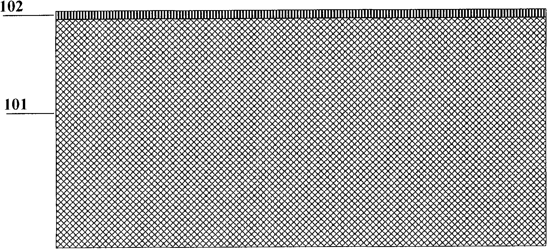
[0033] 1) if Figure 1a As shown, at 950 °C, thermal oxidation growth of SiO 2 thickness of (102);

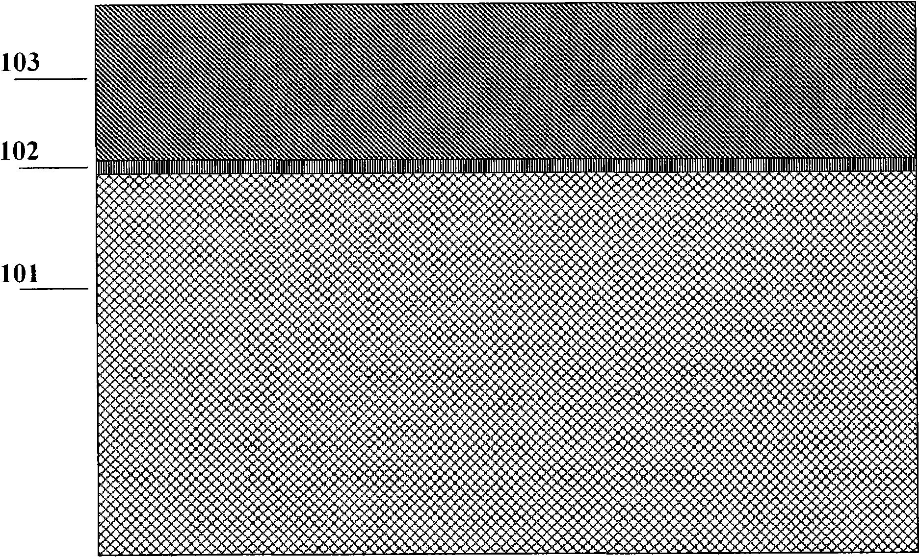
[0034] 2) if Figure 1b As shown, the low pressure chemical vapor deposition polysilicon (103);

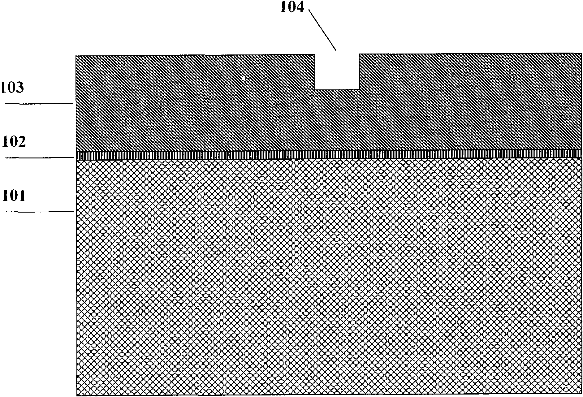
[0035] 3) if Figure 1c Shown, using positive electron beam photoresist ZEP520 exposure. The steep grooves (104) are etched using chlorine-based reactive ions. The etched groove has a width of 100nm and a depth of 10nm;

[0036] 4) Chemical vapor deposition oxide dielectric layer LTO (105), with a thickness of 30nm;

[0037] 5) if Figure 1d As shown, the surface of the oxide dielectric layer is planarized (105) by chemical mechanical sectioning.

[0038] 6) If Figure 1e As shown, a positive electron beam photoresist ZEP520 is used to expose two grooves ( 107 ) with a defined pitch of 80 nm. The steep grooves are etched using fluorine-based reactive ions. The etched groove has a width of 100 nm and a depth of 10 nm.

[0039] 7) if Figure 1f As shown, the oxide la...


PUM

PropertyMeasurementUnit
Widthaaaaaaaaaa
Depthaaaaaaaaaa
Thicknessaaaaaaaaaa

Abstract

A method for realizing a sub-10nm gate length line is provided by the present invention, comprising the following steps that: a dielectric layer is formed on a substrate in a deposition way or a thermal oxide growth manner; gate electrode materials are deposited; a positive electron beam exposure is carried out and a groove is etched; an oxide dielectric layer is deposited; planarization of the oxide dielectric layer surface is carried out; the positive electron beam exposure is carried out and grooves are etched; and the gate electrode materials and the like are etched. The method in the present invention has a simple process and a good repeatability, a traditional top to down process is completely employed to realize complete compatibility with a CMOS (Complementary Metal Oxide Semiconductor) process, and a process window is large and easy to integrate, which is in favor of defining an extreme short fine graph in a microelectronic process flow, thereby making the minimum characteristic dimension not rely on lithography capability, and promoting device dimension to develop in the direction of smaller dimension.

Description

technical field [0001] The invention belongs to the field of micro-electronic and nano-scale micro-nano electronic devices, in particular to a method for defining fine grid line patterns when preparing semiconductor devices. Background technique [0002] With the development of micro-nano electronics technology, it becomes more and more difficult to define extremely fine lines during the fabrication process. Even if resolution enhancement techniques such as phase shift mask (PSM) and optical proximity correction (OPC) are adopted, the limit resolution of ordinary optical lithography can only reach 1 / 2 of the wavelength of the light source, and the light entering the deep ultraviolet region The wavelength limit is only 193nm, so to achieve sub-10nm line exposure requires more advanced technology. [0003] Using electron beam exposure, by optimizing the process conditions, using expensive photoresist with high exposure dose (such as HSQ, etc.), assisting other technologies (s...

Claims


Application Information

Patent Timeline
IPC IPC(8): H01L21/28
Inventor 宋毅徐秋霞周华杰
Owner INST OF MICROELECTRONICS CHINESE ACAD OF SCI
Learn More