Semiconductor ultraviolet detection sensor and preparation method thereof

A semiconductor and sensor technology, applied in the field of ultraviolet light detection, can solve the problems of zinc oxide nanowires exposed to the air for a long time, and achieve the effect of improving the photoresponse current value, good repeatability and low price

Inactive Publication Date: 2011-06-29
LANZHOU UNIVERSITY
View PDF2 Cites 25 Cited by
  • Summary
  • Abstract
  • Description
  • Claims
  • Application Information

AI Technical Summary

Problems solved by technology

It can be seen from the patent application documents that theoretically extending the length of the electrode and integrating more zinc oxide nanowires on the electrode may further increase the photoresponse current value, but in practice this approach is not feasible because the receiving device The size limit cannot extend the length of the electrode without limit so that more zinc oxide nanowires can be integrated between the electrodes
On the other hand, this technology also has the disadvantage that zinc oxide nanowires are exposed to air for a long time.

Method used


Image

  • Semiconductor ultraviolet detection sensor and preparation method thereof
  • Semiconductor ultraviolet detection sensor and preparation method thereof
  • Semiconductor ultraviolet detection sensor and preparation method thereof

Examples


Embodiment 1

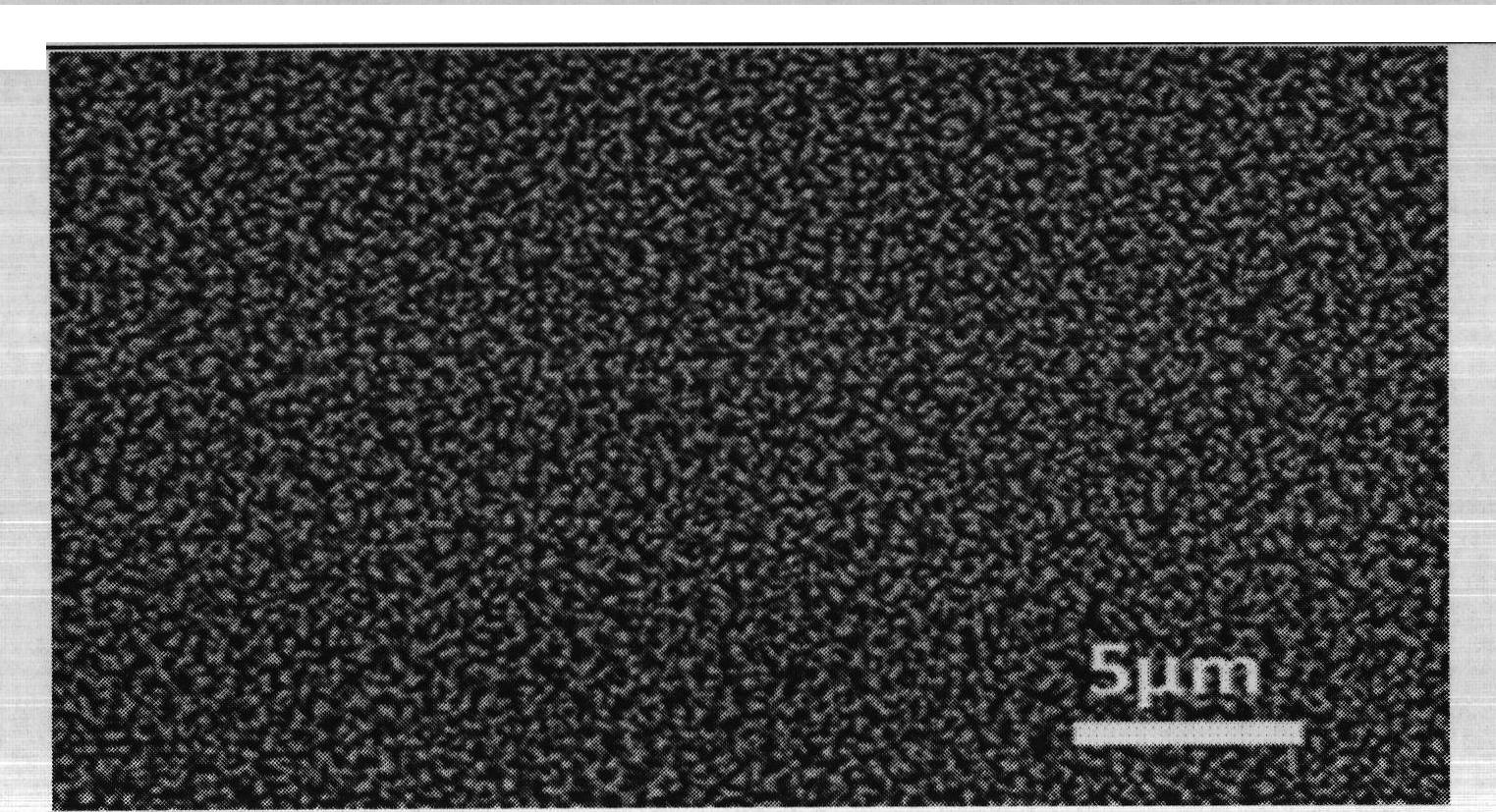
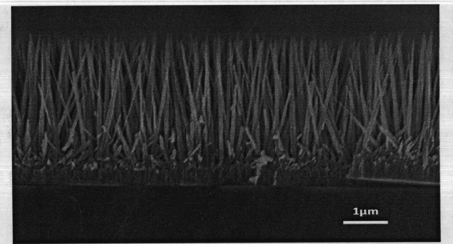
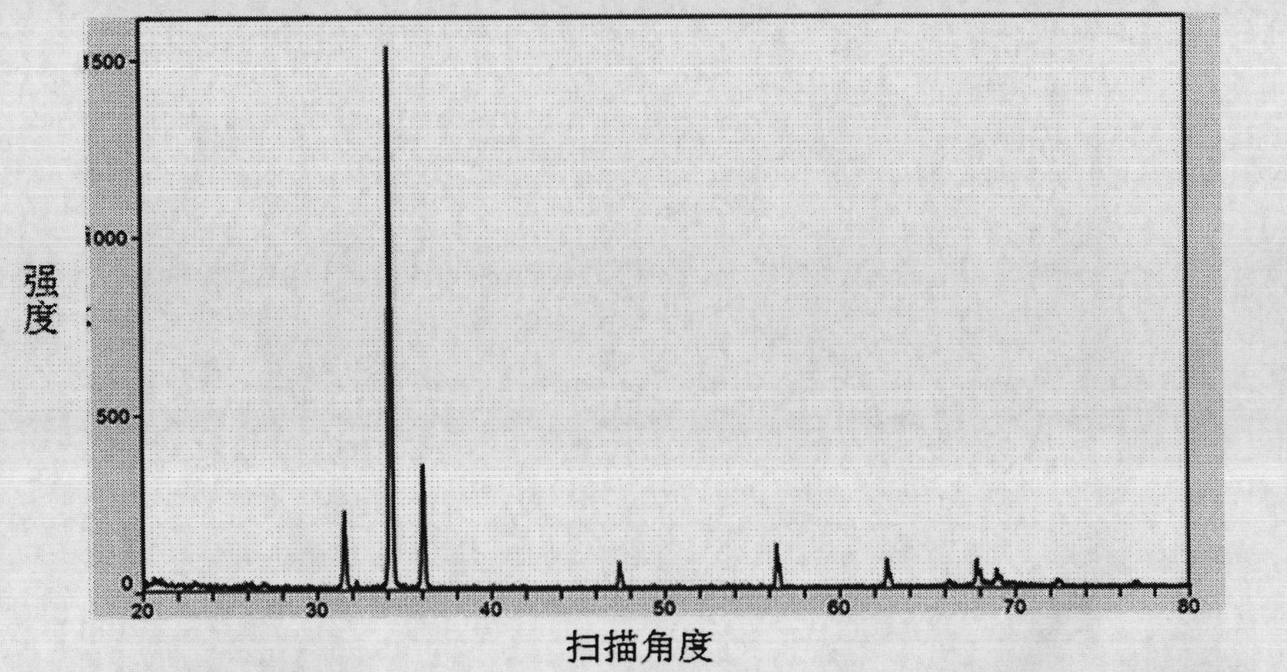
[0039] 1. At first adopt the high-temperature chemical vapor deposition method or hydrothermal method to grow the zinc oxide nanowire array perpendicular to the substrate on the substrate, the substrate used in the present invention is a silicon wafer, the zinc oxide nanowire array grown on the substrate For morphology and characterization, see the appendix figure 1 , attached figure 2 And attached image 3 .

[0040] When preparing by high temperature chemical vapor deposition, the mixture of ground 0.81g zinc oxide and 0.12g graphite powder is put into the reaction boat, and the reaction boat is put into the closed end of the single opening sleeve. Cut the silicon wafer whose polished surface is (100) crystal plane into small pieces of 0.5cm×0.8cm, ultrasonically clean them with HF, acetone, absolute ethanol and distilled water successively for 20 minutes, and blow dry the surface of the silicon wafer with nitrogen after taking it out. Bake in an oven at 175°C for 1 hour...

Embodiment 2

[0059] Example 2: Preparation of a high-response ultraviolet light sensor with non-hermetically sealed ohmic contacts

[0060] Spin-coat a layer of photoresist on the glass sheet, and the speed of the spinner is changed from slow to fast, and the final speed is 3000 rpm, and the speed is maintained for 60 seconds. Then pre-baked in an oven at 90 degrees Celsius for 40 minutes, then exposed the electrode pattern on the mask plate to the glass sheet under the microscope of the photolithography machine, and then baked it at 110 degrees Celsius for 30 minutes, and made an insertion with a width of 10 μm after development. Photolithographic pattern of half of the finger electrodes. Magnetron sputtering a layer of zinc oxide film with a thickness of about 300-4000nm, and then sputtering a layer of chromium barrier layer on the zinc oxide film (or not combined with Zn(NO 3 ) 2 Other metals that react with HMTA), the thickness is about 10-100nm. After stripping, a comb-tooth electr...


PUM


Abstract

The invention discloses a semiconductor sensor for ultraviolet detection and a preparation method of the sensor. The semiconductor ultraviolet detection sensor comprises a baseplate, electrodes loaded on the baseplate and zinc oxide nanowires which are positioned between the electrodes, connected in parallel and integrated, wherein the electrodes are two comb tooth-shaped electrodes which are arranged oppositely, one comb tooth of one electrode is inserted between two comb teeth of the other electrode so as to form the tooth insertion shape, and the zinc oxide nanowires are respectively connected in parallel and integrated on the adjacent two comb teeth. The light response current of the semiconductor ultraviolet detection sensor can achieve the milliamp magnitude, thereby significantly reducing the ultraviolet detection difficulty and the characterization difficulty of the strength thereof.

Description

technical field [0001] The invention discloses a semiconductor sensor for ultraviolet detection and a preparation method of the sensor, belonging to the technical category of ultraviolet light detection. The semiconductor ultraviolet detection sensor of the invention is an integrated ultraviolet light detector using zinc oxide nanowire arrays. Background technique [0002] As a dual-use technology with broad application prospects, ultraviolet detection has begun a lot of research and application in the late 1980s. In terms of military affairs, the U.S. Navy’s C-130S helicopter and P-3S transport aircraft that were put into use in the Gulf War in 1991 had the world’s first ultraviolet warning device AAR-47, and the United States continued to invest manpower and material resources in research and development of ultraviolet light. Sensor Technology. Recently, only the Magnolia Optical Technology Company has received 1.25 million US dollars of funding for research in this area...

Claims


Application Information

Patent Timeline
Patent Type & Authority Applications(China)
IPC IPC(8): H01L31/09G01J1/42H01L31/0224H01L31/0203H01L31/18
CPCY02P70/50
Inventor 秦勇白所吴巍炜
Owner LANZHOU UNIVERSITY
Why Eureka
Try Eureka