Organic floating gate field effect transistor and preparation method thereof

A technology of field effect transistors and floating gates, which is applied in the field of organic floating gate field effect transistors and its preparation, and can solve problems that cannot be solved well

Inactive Publication Date: 2012-12-12
DALIAN JIAOTONG UNIVERSITY
View PDF0 Cites 0 Cited by
  • Summary
  • Abstract
  • Description
  • Claims
  • Application Information

AI Technical Summary

Problems solved by technology

Organic floating gate field-effect transistors used in gas detectors (M.A.Reyes-Barranca, et al, Materials 21(3)5-9, September 2008) and PH environmental tests, such as S.William et al. in the UK, study the memory of organic devices function (S.William, etal, Applied physics letters 95, 093309, 2009.) and the relationship between the capacitance and voltage of the insulating layer, but the above-mentioned device structure and experimental results cannot well solve the problems raised above

Method used


Image

  • Organic floating gate field effect transistor and preparation method thereof
  • Organic floating gate field effect transistor and preparation method thereof
  • Organic floating gate field effect transistor and preparation method thereof

Examples


preparation example Construction

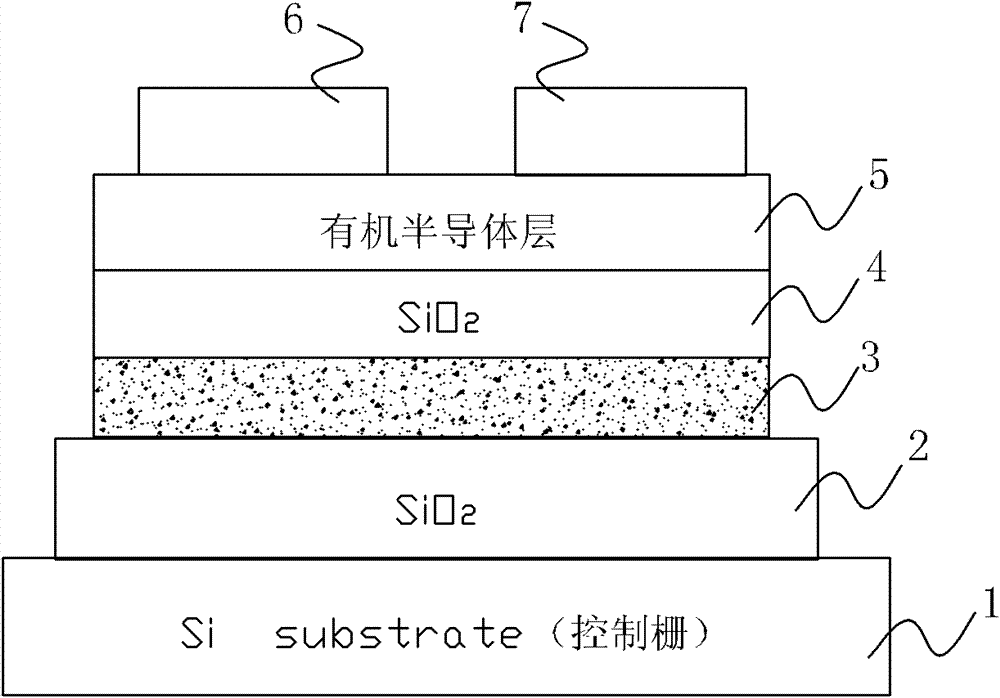
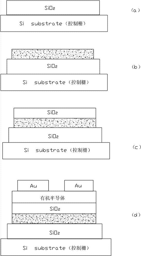
[0025] Such as image 3 The method for preparing the organic floating gate field effect transistor includes the following steps:

[0026] ①. On the silicon substrate 1, a layer of silicon dioxide film is grown as the insulating layer I 2 by the method of thermal oxidation; see the attached image 3 .(a)

[0027] 2. Prepare a low-resistance silicon film as the floating gate 3 on the silicon dioxide film layer, i.e. the insulating layer 1 , by magnetron sputtering; image 3 .(b)

[0028] ③. On the 3rd layer of the floating gate, grow a thin layer of silicon dioxide as the insulating layer II4 by means of thermal oxidation; see attached image 3 .(c)

[0029] ④, then vacuum thermally evaporate a layer of organic semiconductor thin film material on the insulating layer II4 to form the semiconductor active layer 5;

[0030] 5. Vacuum heat evaporation of one layer of gold thin film layer on the semiconductor active layer 5 is used as the electrode material of the device;

[00...

Embodiment

[0034] Such as image 3 As shown, a layer of silicon dioxide insulating layer I2 is prepared on the polysilicon substrate 1 by thermal oxidation (dry oxygen oxidation method), the conditions are: the oxidation temperature is 1200 degrees Celsius, and the dry oxygen oxidation time is about 1 hour, and then use Prepare a layer of silicon film (floating gate 3) on the silicon dioxide insulating layer by magnetron sputtering (sputtering conditions are sputtering power 250W, background vacuum degree 1.5×10 -4 Pa, Ar gas pressure 1Pa. ), the thickness of the silicon film is about 20nm. Then prepare a layer of silicon dioxide insulating layer II4 by thermal oxidation (dry oxygen), the conditions are: the preparation environment is 1200 degrees Celsius, dry oxygen for 5 minutes, and the thickness of the obtained silicon dioxide is about ten nanometers. Then adopt the method for vacuum thermal evaporation to prepare organic semiconductor material (form semiconductor active layer 5), ...


PUM


Abstract

The invention discloses an organic floating gate field effect transistor and a preparation method thereof, and is characterized in that: the transistor consists of a substrate, an insulating layer I formed on the substrate, a floating gate formed on the insulating layer I, an insulating layer II formed on the floating gate, a semiconductor active layer formed on the insulating layer II, and a source electrode and a drain electrode which are formed on the semiconductor active layer. The preparation method of the organic floating gate field effect transistor comprises the following steps of: (1) growing one insulating layer I on a silicon substrate; (2) preparing a low-resistance silicon film which serves as the floating gate on the insulating layer I by a magnetron sputtering method; (3) growing one insulating layer II on a floating gate layer by a thermal oxidation method; (4) performing vacuum thermal evaporation to form one semiconductor active layer made of an organic semiconductorfilm material on the insulating layer II; (5) performing vacuum thermal evaporation to form one gold film layer which serves as an electrode material of the device on the semiconductor active layer; and (6) performing photoetching on the electrode material to obtain the source electrode and the drain electrode. By the transistor, the information energy of the floating gate can be effectively controlled to be erased.

Description

technical field [0001] The invention relates to an organic floating gate field effect transistor and a preparation method thereof. Background technique [0002] The floating gate field effect transistor is the core device of the integrated circuit storage part, and its usual structure (attached figure 1 ) is to add a layer of floating gate to the insulating layer of ordinary field effect transistors to change the threshold voltage of the device and realize the function of information storage. At present, the floating gate field effect transistor of silicon semiconductor structure mostly adopts the large-scale integrated circuit production process, usually grows multi-layer films on the silicon wafer, and performs photolithography, ion implantation, etching and other operations on the film to obtain the floating gate field effect transistor. It has the advantages of high integration and good reliability, but also has the disadvantages of complicated production, high producti...

Claims


Application Information

Patent Timeline
Patent Type & Authority Patents(China)
IPC IPC(8): H01L51/05H01L51/40
Inventor 刘向薛钰芝林纪宁周丽梅王颖
Owner DALIAN JIAOTONG UNIVERSITY
Why Eureka
Try Eureka