Nanometer composite multilayer phase change thin-film material for phase change memory

A phase-change memory and nanocomposite technology, which is applied in the field of nanocomposite multilayer phase-change thin film materials, can solve the problems of poor thermal stability and high power consumption of device unit operations, and achieve high crystallization temperature, good amorphous thermal stability, The effect of good thermal stability

Inactive Publication Date: 2011-07-06
TONGJI UNIV
View PDF2 Cites 16 Cited by
  • Summary
  • Abstract
  • Description
  • Claims
  • Application Information

AI Technical Summary

Problems solved by technology

[0003] The phase change material widely used in phase change memory is GeTe-Sb 2 Te 3 Pseudo-binary compounds, where for the component Ge 2 Sb 2 Te 5 (GST) is the most researched, but GST

Method used


Image

  • Nanometer composite multilayer phase change thin-film material for phase change memory
  • Nanometer composite multilayer phase change thin-film material for phase change memory
  • Nanometer composite multilayer phase change thin-film material for phase change memory

Examples


Embodiment 1

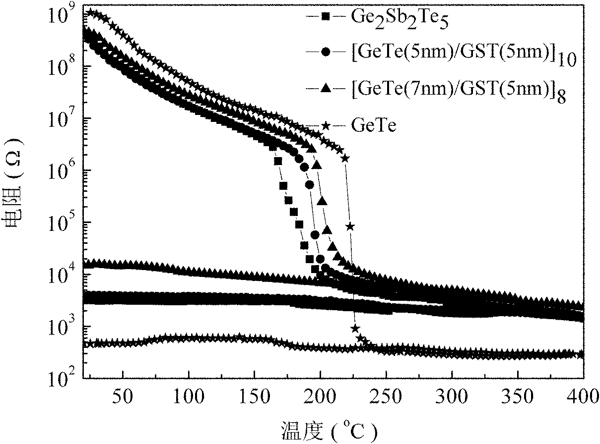
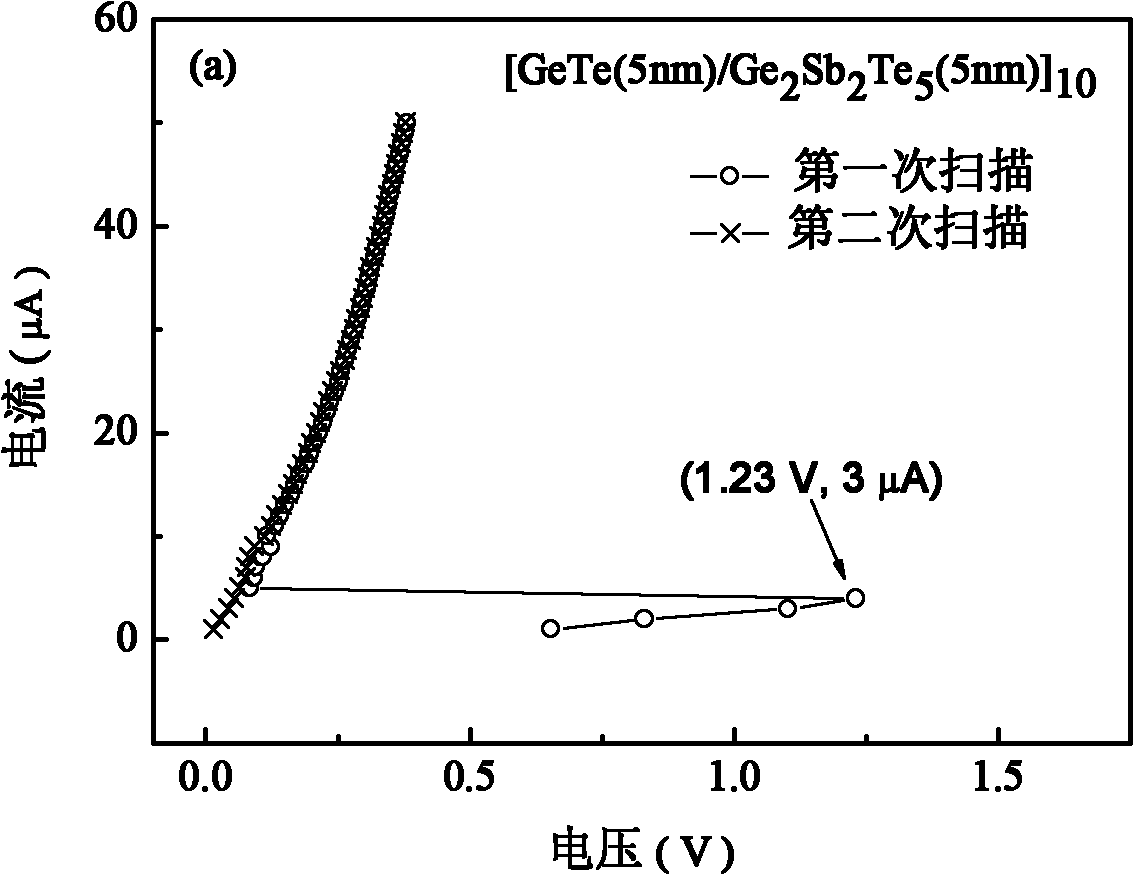
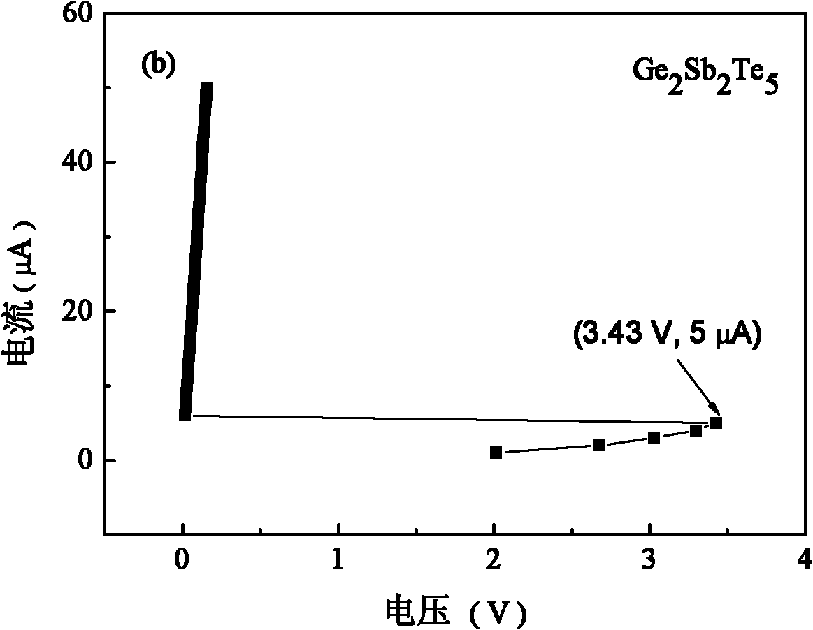
[0041] Prepare GeTe / Ge with the following structure 2 Sb 2 Te 5 Nanocomposite multilayer phase change film material, the structure of the film material is specifically [GeTe(5nm) / Ge 2 Sb 2 Te 5 (5nm)] 10 and [GeTe(7nm) / Ge 2 Sb 2 Te 5 (5nm)] 8 , and the GeTe / Ge 2 Sb 2 Te 5 The total thickness of the nanocomposite multilayer phase change film material is 100nm.

[0042] Concrete preparation steps are as follows:

[0043] 1) Clean SiO2 2 / Si(100) substrate: clean the surface and back, remove dust particles, organic and inorganic impurities; strong ultrasonic cleaning in acetone solution for 3-5 minutes, rinse with deionized water; then strong ultrasonic cleaning in ethanol solution for 3-5 minutes, rinse with deionized water, high-purity N 2 Dry the surface and back; dry the water vapor in an oven at 120°C for about 20 minutes;

[0044] 2) Install the sputtering target: set the radio frequency power, set the sputtering gas flow rate and sputtering pressure;

[00...

Embodiment 2

[0067] The prepared structures are [GeTe(15nm) / Ge 2 Sb 2 Te 5 (5nm)] 5 、[GeTe(5nm) / Ge 2 Sb 2 Te 5 (1nm)] 17 、[GeTe(1nm) / Ge 2 Sb 2 Te 5 (15nm)] 6 and [GeTe(1nm) / Ge 2 Sb 2 Te 5 (5nm)] 17 GeTe / Ge 2 Sb 2 Te 5 Nanocomposite multilayer phase change thin film material, and the GeTe / Ge 2 Sb 2 Te 5 The total thickness of the nanocomposite multilayer phase change thin film material is 100nm, 102nm, 96nm and 102nm respectively.

[0068] Concrete preparation steps are as follows:

[0069] 1) Clean SiO2 2 / Si(100) substrate: clean the surface and back, remove dust particles, organic and inorganic impurities; strong ultrasonic cleaning in acetone solution for 3-5 minutes, rinse with deionized water; then strong ultrasonic cleaning in ethanol solution for 3-5 minutes, rinse with deionized water, high-purity N 2 Dry the surface and back; dry the water vapor in an oven at 120°C for about 20 minutes;

[0070] 2) Install the sputtering target: set the radio frequency powe...

Embodiment 3

[0077] The prepared structure is [GeTe(5nm) / Ge 2 Sb 2 Te 5 (5nm)] 10 GeTe / Ge 2 Sb 2 Te 5 Nanocomposite multilayer phase change thin film material, and the GeTe / Ge 2 Sb 2 Te 5 The total thickness of the nanocomposite multilayer phase change film material is 100nm.

[0078] Concrete preparation steps are as follows:

[0079] 1) Clean SiO2 2 / Si(100) substrate: clean the surface and back, remove dust particles, organic and inorganic impurities; strong ultrasonic cleaning in acetone solution for 3-5 minutes, rinse with deionized water; then strong ultrasonic cleaning in ethanol solution for 3-5 minutes, rinse with deionized water, high-purity N 2 Dry the surface and back; dry the water vapor in an oven at 120°C for about 20 minutes;

[0080] 2) Install the sputtering target: set the radio frequency power, set the sputtering gas flow rate and sputtering pressure;

[0081] Preparation of GeTe / Ge by Magnetron Alternating Sputtering at Room Temperature 2 Sb 2 Te 5 Nano...


PUM

PropertyMeasurementUnit
Thicknessaaaaaaaaaa
Thicknessaaaaaaaaaa

Abstract

The invention belongs to the technical field of microelectronic materials and relates to a nanometer composite multilayer phase change thin-film material for a phase change memory. In a GeTe/Ge2Sb2Te5 nanometer composite multilayer phase change thin-film material, a monolayer GeTe thin film and a monolayer Ge2Sb2Te5 thin film are alternately arranged to form a multilayer thin-film structure, wherein the thicknesses of the monolayer GeTe thin film and the monolayer Ge2Sb2Te5 thin film are both 1-15nm. In the invention, the crystallization temperature of the thin-film material is raised along with the increase of the thickness of the monolayer Ge2Sb2Te5 thin film in the cycle; a reversible transformation between a high resistance state and a low resistance state can be realized through an electrical pulse by utilizing a phase change memory cell based on the GeTe/Ge2Sb2Te5 nanometer composite multilayer phase change thin-film material; and compared with the Ge2Sb2Te5 material, the nanometer composite multilayer phase change thin-film material has higher crystallization temperature, better heat stability in an amorphous state and lower device operation voltage, thereby having lower power consumption.

Description

technical field [0001] The invention belongs to the technical field of microelectronic materials, and relates to a nano-composite multilayer phase-change film material used for a phase-change memory. Background technique [0002] Phase change memory (PCM) has the advantages of high speed, high reliability, low power consumption, long cycle life, etc., and has excellent feature size reduction capabilities, making PCM very likely to replace the current FLASH and become the most mainstream product in the future non-volatile memory technology market. one of the competitors. The operating principle of phase change memory is based on the reversible phase transition of chalcogenide alloy thin films between crystalline and amorphous states under the excitation of an electric field. The crystalline and amorphous states of these materials have greatly different resistivities, corresponding to the binary digits. "1" and "0". [0003] The phase change material widely used in phase cha...

Claims


Application Information

Patent Timeline
IPC IPC(8): H01L45/00B32B9/00B82Y30/00B82Y10/00
Inventor 翟继卫汪昌州沈波孙明成
Owner TONGJI UNIV
Why Eureka
Try Eureka