Method for manufacturing silicon-doped indium arsenide/gallium arsenide quantum-dot solar cell

A technology of solar cells and production methods, which can be applied in the directions of circuits, electrical components, and final product manufacturing, etc., can solve problems such as hindering large-scale popularization and use, and high cost of solar cells.

Inactive Publication Date: 2011-07-20
INST OF SEMICONDUCTORS - CHINESE ACAD OF SCI
View PDF2 Cites 4 Cited by
  • Summary
  • Abstract
  • Description
  • Claims
  • Application Information

AI Technical Summary

Problems solved by technology

However, due to the high cost of current solar cells, it has seriously hindered its large-scale promotion and use.

Method used


Image

  • Method for manufacturing silicon-doped indium arsenide/gallium arsenide quantum-dot solar cell
  • Method for manufacturing silicon-doped indium arsenide/gallium arsenide quantum-dot solar cell

Examples


Embodiment Construction

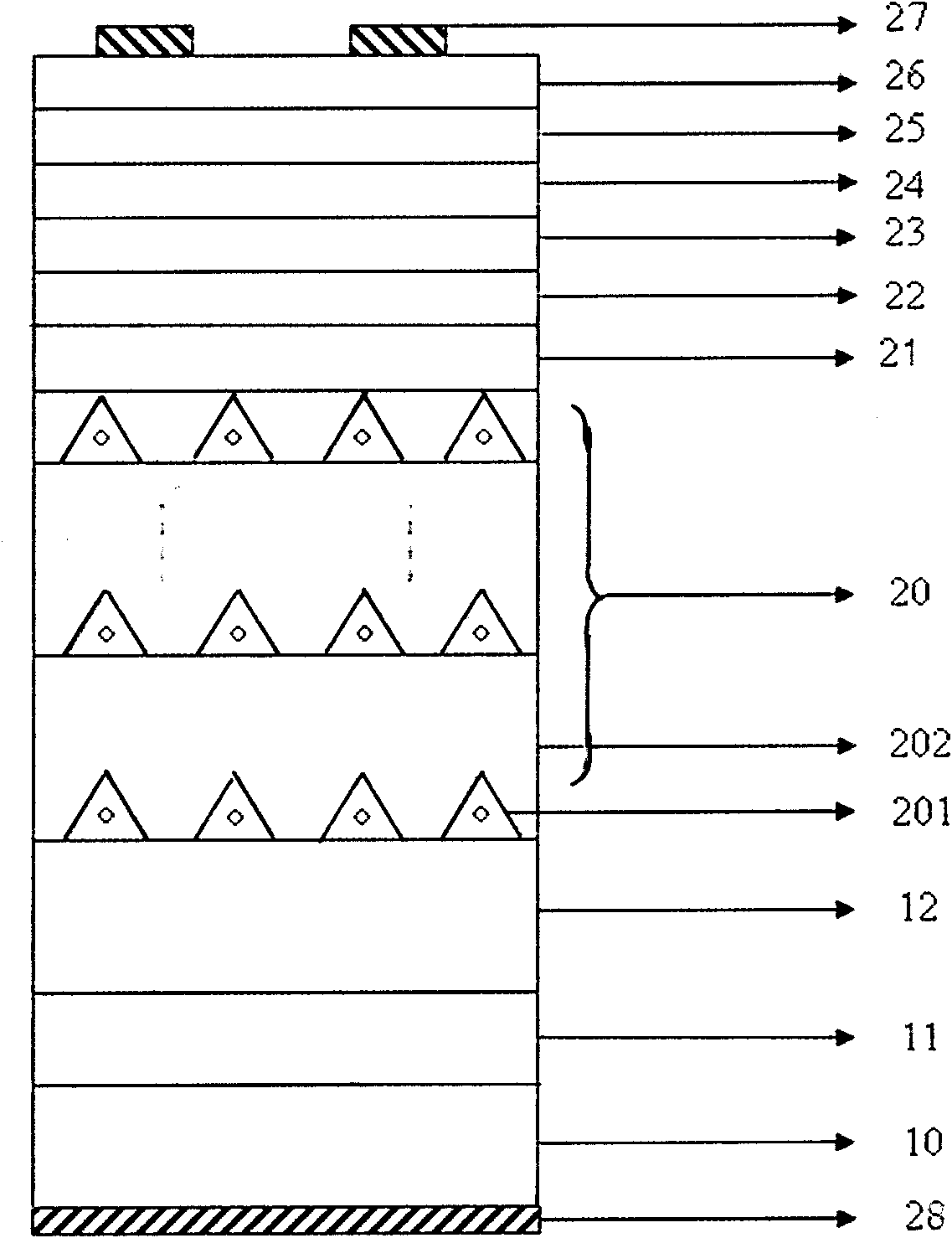
[0022] see figure 1 As shown, the present invention relates to a method for making a silicon-doped indium arsenide / gallium arsenide quantum dot solar cell, comprising the steps of:

[0023] Step 1: Select an n+ type GaAs single wafer 10 as the substrate, and the doping concentration is (0.6-1.4)*10 18 cm -3 ;

[0024] Step 2: grow an n-type GaAs layer 11 on the substrate 10 with a thickness of 500 nm, a growth temperature of 595° C., and a doping concentration of 1.0*10 18 cm -3 ; growing an intrinsic GaAs buffer layer 12 on the n-type GaAs layer 11 with a thickness of 400 nm and a growth temperature of 595° C.;

[0025] Step 3: growing multiple periods of quantum dot structures 20 on the intrinsic GaAs buffer layer 12, as the i absorbing layer of the solar cell, each period of the multiple periods of quantum dot structures 20 includes:

[0026] A silicon-doped InAs quantum dot layer 201 and a GaAs spacer layer 202 are grown sequentially from bottom to top; the number of ...


PUM


Abstract

The invention relates to a method for manufacturing a silicon-doped indium arsenide / gallium arsenide quantum-dot solar cell, comprising the steps of: 1, selecting an n+ type GaAs single chip to serve as a substrate; 2, sequentially growing an n type GaAs layer and an intrinsic GaAs buffer layer on the n+ type GaAs single chip; 3, growing a multi-cycle quantum dot structure to server as an i absorption layer of the cell on the intrinsic GaAs buffer layer; 4, sequentially growing an intrinsic GaAs layer, a p type GaAs layer, a p+ type GaAs layer, a p type A10.4Ga0.6As layer and a p type GaAs layer on the multi-cycle quantum dot structure; 5, growing a ZnS / MgF2 layer on the p type GaAs layer; 6, growing and manufacturing an upper metal electrode on the ZnS / MgF2 layer; 7, manufacturing a lower metal electrode on the lower surface of the n+ type GaAs single chip; and 8, packaging a solar assembly to complete the manufacturing the solar cell.

Description

technical field [0001] The invention belongs to the technical field of photovoltaic device manufacture, and in particular relates to the manufacture of a silicon-doped indium arsenide / gallium arsenide quantum dot solar cell. Background technique [0002] Solar cells are an effective form of clean and renewable energy solar energy, which has aroused great interest from governments, enterprises and research institutions in recent years. In today's increasingly serious greenhouse effect, solar cells with zero carbon emissions are particularly important for protecting the earth's environment and maintaining the sustainable development of the national economy. However, the high cost of the current solar cell seriously hinders its large-scale promotion and use. Improving the conversion efficiency of solar cells is one of the effective ways to reduce the relative cost. At present, the highest efficiencies of single-junction GaAs and Si solar cells are about 26% and 25% respective...

Claims


Application Information

Patent Timeline
Patent Type & Authority Applications(China)
IPC IPC(8): H01L31/18
CPCY02P70/50
Inventor 王科范杨晓光杨涛王占国
Owner INST OF SEMICONDUCTORS - CHINESE ACAD OF SCI
Why Eureka
Try Eureka