

Method for realizing self-assembly of zinc oxide nanometer wires
A zinc oxide nanowire and self-assembly technology, applied in the field of nano-processing, can solve problems affecting the performance of thin-film devices, lack of nanowire films, and nanowire films that are not suitable for manufacturing devices.
- Summary
- Abstract
- Description
- Claims
- Application Information
AI Technical Summary
Problems solved by technology
Method used
Image

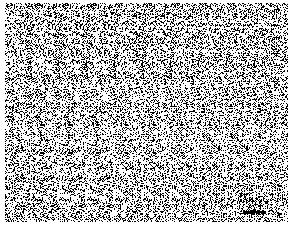
Examples
Embodiment 1
[0019] The first step is to clean the silicon wafer. First, put the silicon wafer with the silicon dioxide insulating layer into 50 ml of ethanol, perform ultrasonic cleaning for 10 minutes, take it out and blow dry with nitrogen; then, put the silicon wafer in 50 ml of acetone and perform ultrasonic cleaning for 10 minutes. Take it out and blow dry with nitrogen; finally put the silicon wafer into 100 ml of deionized water for ultrasonic cleaning for 10 minutes, take it out and blow dry with nitrogen.
[0020] The second step is the hydroxylation of the silicon wafer surface. Prepare a solution with a volume ratio of sulfuric acid (98% concentration) and hydrogen peroxide (30% concentration) at a volume ratio of 2.5:1, put the cleaned silicon wafers into the solution, and cook at 90°C for 2.5 hours. After cooking, put the silicon wafers Take it out and wash it repeatedly with deionized water. Finally, put the silicon wafer into deionized water, boil it at 80°C for 20 minutes, ...
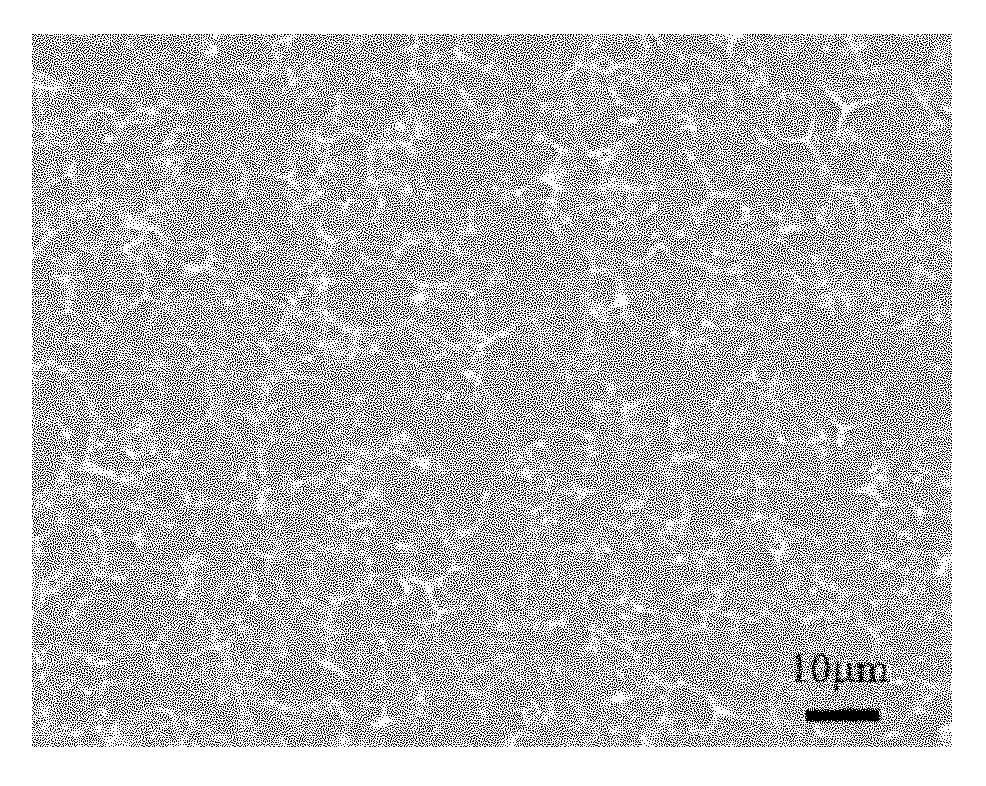
Embodiment 2
[0025] The first step is to clean the silicon wafer. First, put the silicon wafer with the silicon dioxide insulating layer into 50 ml of ethanol, perform ultrasonic cleaning for 10 minutes, take it out and blow dry with nitrogen; then, put the silicon wafer in 50 ml of acetone and perform ultrasonic cleaning for 10 minutes. Take it out and blow dry with nitrogen; finally put the silicon wafer into 100 ml of deionized water for ultrasonic cleaning for 10 minutes, take it out and blow dry with nitrogen.
[0026] The second step is the hydroxylation of the silicon wafer surface. Prepare a solution with a volume ratio of sulfuric acid (98% concentration) and hydrogen peroxide (30% concentration) in a volume ratio of 2.5:1, put the cleaned silicon wafers into the solution, and cook at 90°C for 2 hours. After cooking, put the silicon wafers Take it out and wash it repeatedly with deionized water. Finally, put the cleaned silicon wafer into deionized water, boil it at 80°C for 25 min...
Embodiment 3
[0031] The first step is to clean the silicon wafer. First, put the silicon wafer with the silicon dioxide insulating layer into 50 ml of ethanol, perform ultrasonic cleaning for 10 minutes, take it out and blow dry with nitrogen; then, put the silicon wafer in 50 ml of acetone and perform ultrasonic cleaning for 10 minutes. Take it out and blow dry with nitrogen; finally put the silicon wafer into 100 ml of deionized water for ultrasonic cleaning for 10 minutes, take it out and blow dry with nitrogen.
[0032] The second step is the hydroxylation of the silicon wafer surface. Prepare a solution with a volume ratio of sulfuric acid (98% concentration) and hydrogen peroxide (30% concentration) in a volume ratio of 2.5:1, put the cleaned silicon wafers into the solution, and cook at 90°C for 3 hours. After cooking, put the silicon wafers Take it out and wash it repeatedly with deionized water. Finally, put the cleaned silicon wafer into deionized water, boil it at 80°C for 30 min...
PUM
 Abstract
Description
Claims
Application Information