
Non-polar surface GaN epitaxial wafer and preparation method of non-polar surface GaN epitaxial wafer

A non-polar surface, epitaxial wafer technology, applied in chemical instruments and methods, from chemical reactive gases, single crystal growth, etc., can solve the problems of reducing the luminous efficiency of GaN thin films, blue shift of diode luminescence peaks, and many defects. , to achieve the effect of improving quantum efficiency and luminous efficiency

Inactive Publication Date: 2011-08-10
武汉华炬光电有限公司
View PDF8 Cites 3 Cited by
  • Summary
  • Abstract
  • Description
  • Claims
  • Application Information

AI Technical Summary

Problems solved by technology

[0002] At present, the mainstream substrate for the epitaxial growth of GaN thin films in business is c-plane sapphire crystal. Usually, GaN thin films grown on c-plane sapphire substrates are grown along the direction of its polarity axis, that is, the c-axis, and the thin films have spontaneous polarization and compression. The electric polarization effect causes a strong built-in electric field inside the film, which greatly reduces the luminous efficiency of the GaN film
In addition, the polarized electric field also brings a serious problem: as the injection current increases, the peak of the diode's light emission will also undergo a large blue shift.
Although the lattice mismatch and thermal mismatch between sapphire and GaN are relatively large, with the continuous improvement and improvement of sapphire substrate processing technology and GaN epitaxial growth process, the process of epitaxial GaN thin film on sapphire substrate is becoming more and more mature. Commercialization. Craven et al. first reported the growth of non-polar GaN films on r(0112) plane sapphire. Due to the large lattice mismatch, the quality of the grown films was poor and there were many defects (mainly dislocations and stacking faults).

Method used


Image

  • Non-polar surface GaN epitaxial wafer and preparation method of non-polar surface GaN epitaxial wafer
  • Non-polar surface GaN epitaxial wafer and preparation method of non-polar surface GaN epitaxial wafer
  • Non-polar surface GaN epitaxial wafer and preparation method of non-polar surface GaN epitaxial wafer

Examples


Embodiment Construction

[0010] The present invention will be described in further detail below in conjunction with specific embodiments and with reference to the accompanying drawings.

[0011] A method for preparing a non-polar GaN epitaxial wafer comprises the steps of: growing a buffer layer on a substrate; growing an a-plane GaN thin film on the buffer layer; further, the substrate is an r-plane sapphire substrate; further , the buffer layer is Al grown by metal-organic source vapor phase epitaxy 0.15 Ga 0.85 N, wherein the source of Al is trimethylaluminum, the source of gallium is trimethylgallium, and hydrogen is used as a carrier gas; further, when depositing the buffer layer, the growth temperature is 700°C, the V / III ratio is 6000, and the thickness is 20nm .

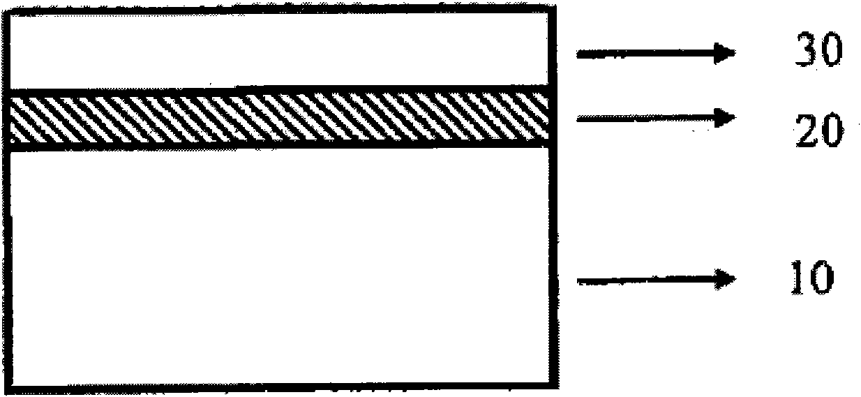
[0012] Please refer to figure 1 , Put the no-clean r-plane single-polished sapphire substrate into the growth chamber of the metal-organic source vapor phase epitaxy (MOCVD) material growth system, slowly raise the temperature to ...


PUM

PropertyMeasurementUnit
mean roughnessaaaaaaaaaa

Abstract

The invention discloses a non-polar surface GaN epitaxial wafer. A non-polar GaN film is synthesized and grown on a sapphire substrate by using a metal organic chemical vapor deposition (MOCVD) system, and the film comprises a low-temperature buffer layer grown on the sapphire at one time and an alpha surface GaN film. Different epitaxial structures of light emitting diodes, laser devices, solar cells and the like are grown on the film in different periods. The growth of the non-polar alpha surface GaN material can be effectively controlled, and the quantum efficiency and the luminous efficiency in the periods can be improved.

Description

technical field [0001] The invention relates to the field of semiconductor material preparation, in particular to a non-polar surface GaN epitaxial wafer and a preparation method thereof. Background technique [0002] At present, the mainstream substrate for the epitaxial growth of GaN thin films in business is c-plane sapphire crystal. Usually, GaN thin films grown on c-plane sapphire substrates are grown along the direction of its polarity axis, that is, the c-axis, and the thin films have spontaneous polarization and compression. The electric polarization effect leads to a strong built-in electric field inside the film, which greatly reduces the luminous efficiency of the GaN film. In addition, the polarization electric field also brings a serious problem: with the increase of the injection current, the luminous peak of the diode will also undergo a large blue shift. [0003] One of the solutions is to grow cubic nitride heterojunctions. Theory shows that there is no sp...

Claims


Application Information

Patent Timeline
Patent Type & Authority Applications(China)
IPC IPC(8): C30B25/02C30B29/38
Inventor 陈莉陈霞熊辉
Owner 武汉华炬光电有限公司
Learn More