Crystalline silicon ingot casting method and silicon ingot

A technology for crystalline silicon and silicon ingots, applied in the field of crystalline silicon ingot casting methods and silicon ingots, can solve the problems of easy complete melting of seed crystals, unrealizable polycrystalline silicon with large grains, and poor temperature control.

Inactive Publication Date: 2011-08-17
JIANGXI SAI WEI LDK SOLAR HI TECH CO LTD
View PDF6 Cites 22 Cited by
  • Summary
  • Abstract
  • Description
  • Claims
  • Application Information

AI Technical Summary

Problems solved by technology

In view of this, the prior art proposes the use of directional solidification to produce monocrystalline silicon or polycrystalline silicon with large grains, thereby improving the conversion efficiency of crystalline silicon and increasing production efficiency to reduce production costs. However, in the prior art, In the method of producing monocrystalline silicon or polycrystalline silicon with large grains by directional solidification, silicon crystals are used as seed crystals to obtain monocrystalline silicon or polycrystalline silicon with large grains. Due to the use of homogeneous silicon crystals as seed crystals, The silicon seed crystal has the same physical properties as the melting point of the homogeneous silicon raw material, and the temperature is not easy to control during ingot casting, and the seed crystal is easy to completely melt, resulting in the production of single crystal silicon or polycrystalline silicon with large crystal grains by directional solidification It cannot be realized, and after the ingot casting is completed, the silicon seed crystal cannot be reused because it is integrated with the silicon ingot and is difficult to separate; every time a silicon seed crystal is used to cast an ingot, a new silicon seed crystal must be made, which increases production The process also increases the production cost

Method used


Image

  • Crystalline silicon ingot casting method and silicon ingot
  • Crystalline silicon ingot casting method and silicon ingot
  • Crystalline silicon ingot casting method and silicon ingot

Examples


Embodiment Construction

[0053] The technical solutions in the embodiments of the present invention will be clarified below in conjunction with the accompanying drawings in the embodiments of the present invention

[0054]Clear and complete description, obviously, the described embodiment is only a part of the embodiment of the present invention, rather than

[0055] Full examples. Based on the embodiments of the present invention, those of ordinary skill in the art have not made any inventions

[0056] All other embodiments obtained under the premise of sexual labor all belong to the protection scope of the present invention.

[0057] In order to make the object, technical solution and advantages of the present invention clearer, the following describes the present invention with reference to the accompanying drawings:

[0058] The examples will be described in further detail.

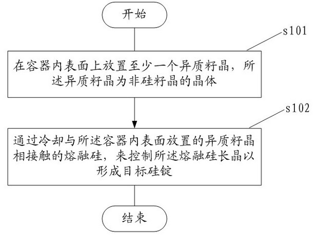
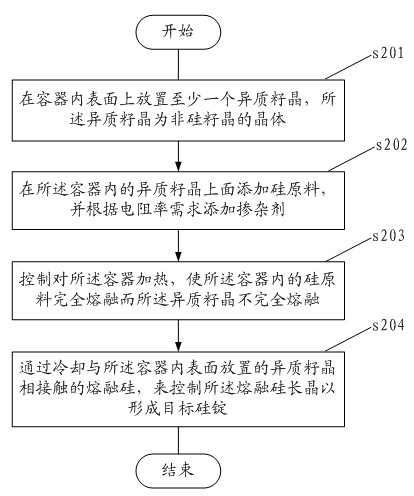
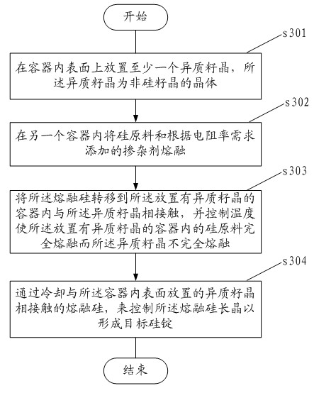
[0059] refer to figure 1 It is a flowchart of the first embodiment of the method for casting crystalline silicon ingots...


PUM


Abstract

The invention discloses a crystalline silicon ingot casting method. The method comprises the following steps of: placing at least one heterogeneous seed crystal on the inner surface of a vessel, wherein the at least one heterogeneous seed crystal is a crystal of a non-silicon seed crystal; and controlling fused silica to grow crystals so as to form a target silicon ingot by cooling the fused silica which is contacted with the at least one heterogeneous seed crystal placed on the inner surface of the vessel. The invention also discloses the silicon ingot, and single crystals or large-grain polycrystalline silicon grow by using non-silicon crystals as the seed crystals in the vessel. The at least one heterogeneous seed crystal and the silicon crystals are substances with different physical and chemical properties, so that the temperature during ingot casting is easy to control to make the at least one heterogeneous seed crystal not completely fused. The aims that the at least one heterogeneous seed crystal is repeatedly used and the production process is simplified are fulfilled by the property that different substances are easy to separate.

Description

technical field [0001] The invention relates to the field of photovoltaics, in particular to a method for casting crystalline silicon ingots and silicon ingots. Background technique [0002] In the fast-growing photovoltaic industry, competition is becoming more and more exciting, and high efficiency and low cost have become the main competition point. The current methods for obtaining the crystalline silicon generally include: the Czochralski (CZ, Czochralski) method and the zone melting (FZ, Float-Zone) method of monocrystalline silicon, and the directional solidification method of polycrystalline silicon. Among them, since the directional solidification method for producing polysilicon produces larger polysilicon ingots each time, the production efficiency is greatly improved, but in conventional polysilicon, grain boundaries will be generated due to dislocations formed on the boundaries between crystal grains, which will As a result, the conversion efficiency of cells p...

Claims


Application Information

Patent Timeline
Patent Type & Authority Applications(China)
IPC IPC(8): C30B11/14C30B29/06C30B28/06
Inventor 钟德京张涛胡动力
Owner JIANGXI SAI WEI LDK SOLAR HI TECH CO LTD
Why Eureka
Try Eureka