IGBT with current carrier storage layer and additional hole passage

A carrier storage and hole technology, applied in circuits, electrical components, semiconductor devices, etc., can solve the problems of overvoltage shock resistance, low anti-interference, high internal resistance of high-voltage IGBTs, and harsh environmental conditions, etc., to achieve optimal circulation Effects of path, opening prevention, safe work area expansion

Inactive Publication Date: 2011-08-17
UNIV OF ELECTRONICS SCI & TECH OF CHINA
View PDF2 Cites 18 Cited by
  • Summary
  • Abstract
  • Description
  • Claims
  • Application Information

AI Technical Summary

Problems solved by technology

The biggest advantage of IGBT is that it can withstand the current impact no matter in the conduction state or in the short circuit state. Its disadvantage is that the internal resistance of the high-voltage IGBT is large, resulting in large conduction loss. Multiple in series, and low tolerance for overvoltage, overheating, impact resistance, anti-interference, etc.
The main characteristic of IGBT is low conduction loss, which can be used in high voltage field. However, in high voltage applications, the environmental conditions are harsh. In addition to excellent conduction characteristics, IGBT needs to have high reliability.

Method used


Image

  • IGBT with current carrier storage layer and additional hole passage
  • IGBT with current carrier storage layer and additional hole passage
  • IGBT with current carrier storage layer and additional hole passage

Examples


Embodiment Construction

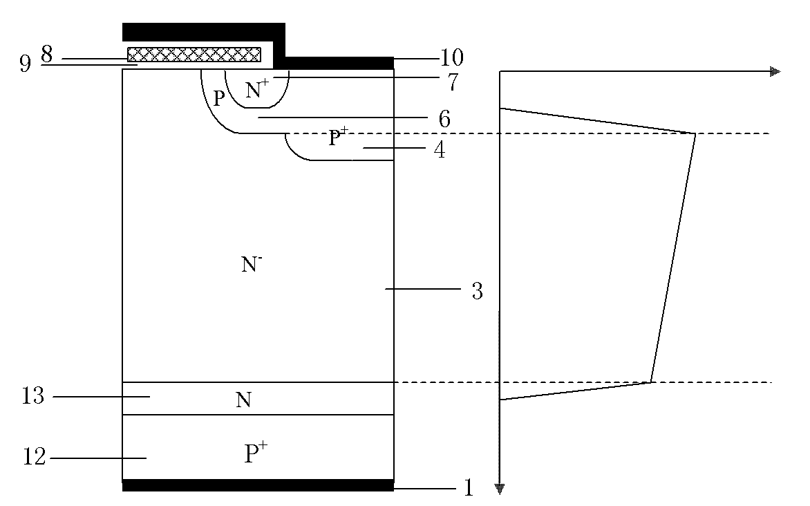
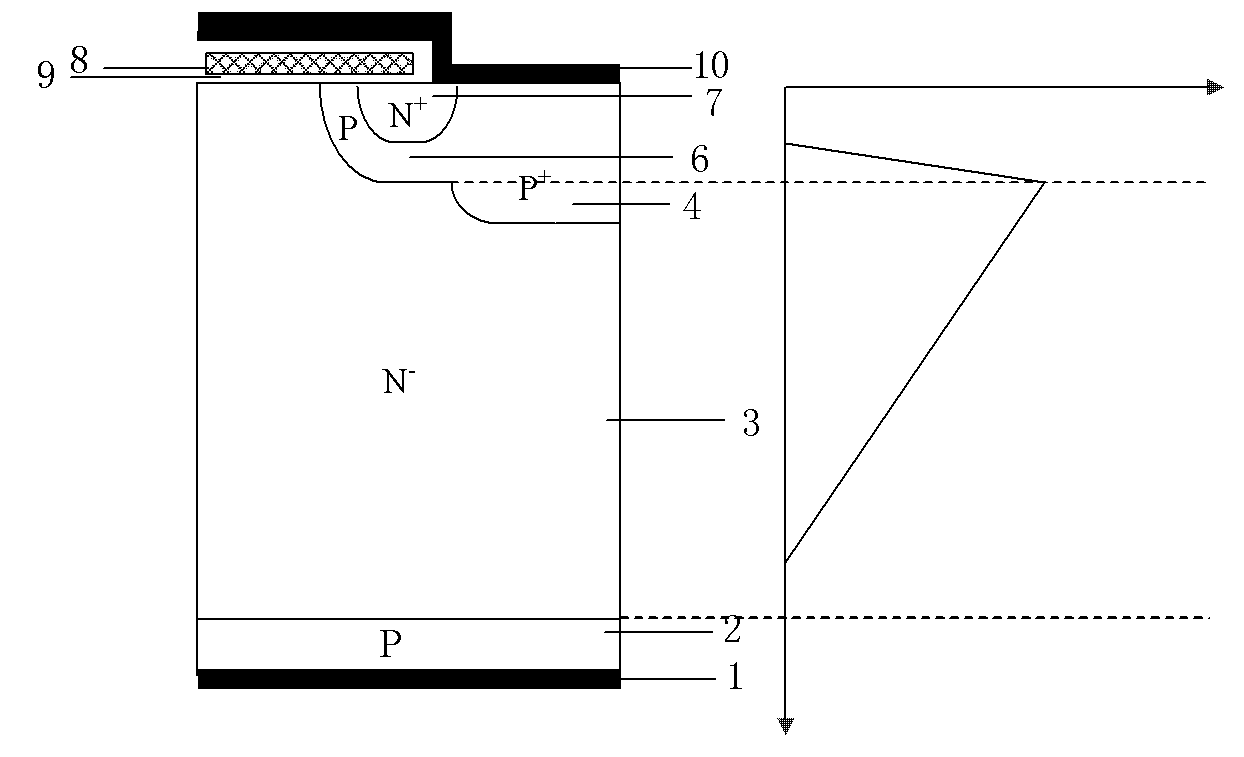
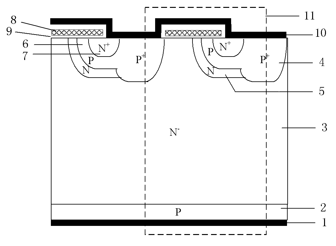
[0032] An IGBT with a carrier storage layer and an additional hole path, such as image 3 As shown, its single cell includes metallized collector electrode 1 on the back of P-type collector region 2, P-type collector region 2, N - Drift zone 3; including those located at N - The top of the drift region 3, the N part in contact with both the metallized emitter 10 and the gate oxide layer 9 + type source region 7, which is in contact with the gate oxide layer 9 and half surrounds the N + The P-type base region 6 of the source region 7; also includes the N-type carrier storage layer 5 that is in contact with the gate oxide layer 9 and half surrounds the P-type base region 6; also includes a P + body region 4, the P + The body region 4 is located below the metallized emitter 10, and the metallized emitter 10, N + Type source region 7, P type base region 6, N type carrier storage layer 5 and N type - P + body region 4; the P + The volume of body region 4 and N + The sum of ...


PUM


Abstract

The invention discloses an insulate gate bipolar transistor (IGBT) with a current carrier storage layer and an additional hole passage, and belongs to the technical field of semiconductor power devices. In the IGBT, an N-type current carrier storage layer (5) and a large P<+> tagma (4) structure are introduced on the basis of a conventional planar non-pouch-through IGBT. The N-type current carrier storage layer (5) improves a conductivity modulation effect close to an emitter and the large P<+> tagma (4) structure plays a role in providing an additional passage for a hole so that the latch-up resistance is improved. Due to the design of the N-type current carrier storage layer (5) and the large P<+> tagma (4), the flow path of a hole current of the conventional IGBT is optimized, so that a safety operation area of a device is enlarged and the sensitivity of latch current density to a temperature is reduced.

Description

technical field [0001] An IGBT with a carrier storage layer and an extra hole path belongs to the technical field of semiconductor power devices. Background technique [0002] IGBT (Insulate Gate Bipolar Transistor) insulated gate bipolar transistor is a new type of power semiconductor device. It has become a new generation of mainstream products in the field of power electronics. It is a combination of MOS and bipolar devices with MOS input and bipolar output functions. Structurally, it is a high-power integrated device composed of thousands of repeating units (ie cells) and manufactured using large-scale integrated circuit technology and power device technology. [0003] IGBT not only has the advantages of high input impedance, low control power, simple driving circuit and high switching speed of MOSFET, but also has the advantages of high current density, low saturation voltage and strong current handling capacity of bipolar power transistor. Therefore, the three major...

Claims


Application Information

Patent Timeline
Patent Type & Authority Applications(China)
IPC IPC(8): H01L29/739H01L29/06
Inventor 李泽宏张超张波
Owner UNIV OF ELECTRONICS SCI & TECH OF CHINA
Why Eureka
Try Eureka