Barrier type silicon-based thin film semi-laminated solar cell

A technology of silicon-based thin film and laminated sun, which is applied in circuits, photovoltaic power generation, electrical components, etc., can solve the problems of increasing spectral absorption, limiting performance stability, and complex manufacturing process

Active Publication Date: 2011-08-17
JIANGSU UNIV
View PDF4 Cites 5 Cited by
  • Summary
  • Abstract
  • Description
  • Claims
  • Application Information

AI Technical Summary

Problems solved by technology

[0002] At present, silicon-based solar cells are mainly monocrystalline silicon, polycrystalline silicon, and thin-film silicon solar cells. Thin-film solar cells are mainly single-junction PIN structures and stacked solar cell structures. Among them, single-junction amorphous silicon cells with PIN structures Although it can absorb more solar spectrum, due to the instability of amorphous silicon, the battery has S-W effect, which limits the stability of its performance, and stacked solar cells have been greatly developed. Hydrogenated amorphous silicon cells As the top cell, the microcrystalline silicon amorphous silicon stacked cell with hydrogenated microcrystalline silicon cell as the bottom cell is a hot spot in current research and application. Although stacked solar cells can make full use of the solar spectrum, it is necessary to increase the thickness of the absorbing layer. At the same time, an intermediate reflective layer or buffer layer is introduced to increase the absorption of light by the intrinsic layer of amorphous silicon, thereby increasing the current, and finally improving the overall performance of the laminated battery. Different combinations of laminated batt

Method used


Image

  • Barrier type silicon-based thin film semi-laminated solar cell
  • Barrier type silicon-based thin film semi-laminated solar cell
  • Barrier type silicon-based thin film semi-laminated solar cell

Examples


Embodiment Construction

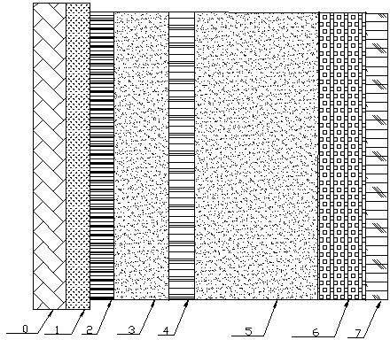
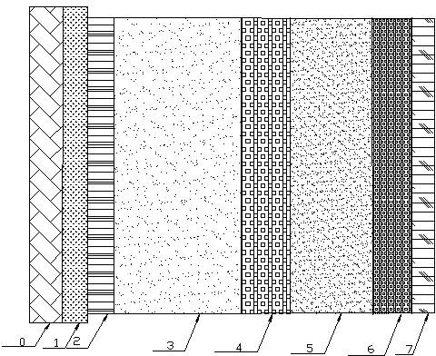
[0026] 1. Structural design of solar cells

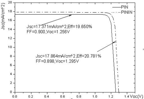
[0027] Deposition of P on a transparent glass substrate 2 I 2 P 1 I 1 N 1 and P 1 I 1 N 1 I 2 N 2 Barrier type semi-stacked thin film solar cells with structure, where P 2 I 2 P 1 I 1 N 1 and P 1 I 1 N 1 I 2 N 2 The optical bandgap Eg of each layer in the P 2 I 2 P 1 I 1 N 1 structure, P 2 The doping concentration is taken as 3.0×10 19 cm -3 , Eg=1.96eV, I 2 Eg=1.8eV, P 1 The doping concentration is 3.0×10 17 cm -3 , Eg=1.96eV, I 1 Eg=1.7eV, N 1 The doping concentration is 3.0×10 19 cm -3 , Eg=1.6eV, at P 1 I 1 N 1 I 2 N 2 structure, P 1 The doping concentration is taken as 3.0×10 19 cm -3 , Eg=1.96eV, I 1 Eg=1.8eV, N 1 The doping concentration is 3.0×10 17 cm -3 , Eg=1.75eV, I 2 Eg=1.7eV, N 2 The doping concentration is 3.0×10 19 cm -3 , Eg=1.6eV, the band gap of each layer decreases in turn, which is conducive to the full absorption of the solar spectrum, thereby improving the ...


PUM

PropertyMeasurementUnit
Bandgap widthaaaaaaaaaa
Thicknessaaaaaaaaaa
Thickness rangeaaaaaaaaaa

Abstract

The invention relates to a silicon-based thin film semi-laminated solar cell, in particular to a barrier type silicon-based thin film semi-laminated solar cell with different doping densities and forbidden band widths on various layers. The barrier type silicon-base thin film semi-laminated solar cell structurally comprises P2I2P1I1N1 and P1I1N1I2N2. The barrier type silicon-based thin film semi-laminated solar cell not only combines the advantages of a laminated cell and a gradually changing band gap thin film cell, but also increases the total thickness of an I layer of a solar cell relative to a PIN structure, thereby providing more places for electron-hole pair generation; the generated photon-generated carriers have enough kinetic energy to move to both anode and cathode of the solarcell by enhancing the effects of P2 and P2 and strengthening a barrier electric field positioned in I, and therefore the short-circuit current and the open-circuit voltage of the solar cell are increased; meanwhile, filling factors and conversion efficiency are greatly enhanced; in addition, matching of an intermediate layer and a buffer layer is not needed, and the excessive interfacial effect of the laminated cell can be reduced.

Description

technical field [0001] The invention relates to a silicon-based thin-film solar cell, in particular to a barrier-type silicon-based thin-film semi-stacked solar cell with different doping concentrations and forbidden band widths of each layer. Background technique [0002] At present, silicon-based solar cells are mainly monocrystalline silicon, polycrystalline silicon, and thin-film silicon solar cells. Thin-film solar cells are mainly single-junction PIN structures and stacked solar cell structures. Among them, single-junction amorphous silicon cells with PIN structures Although it can absorb more solar spectrum, due to the instability of amorphous silicon, the battery has S-W effect, which limits the stability of its performance, and stacked solar cells have been greatly developed. Hydrogenated amorphous silicon cells As the top cell, the microcrystalline silicon amorphous silicon stacked cell with hydrogenated microcrystalline silicon cell as the bottom cell is a hot spo...

Claims


Application Information

Patent Timeline
IPC IPC(8): H01L31/078H01L31/0352H01L31/04
CPCY02E10/50
Inventor 丁建宁卢超郭立强祝俊程广贵林爱国
Owner JIANGSU UNIV
Why Eureka
Try Eureka