Method for manufacturing graphical sapphire substrate

A patterned sapphire and manufacturing method technology, which is applied in the direction of photolithography exposure device, microlithography exposure equipment, electrical components, etc., can solve the problems of low productivity, low pattern consistency, low yield, etc., to avoid damage, Solve the effect of photoresist carbonization

Inactive Publication Date: 2011-08-17
长治虹源科技晶体有限公司
View PDF4 Cites 20 Cited by
  • Summary
  • Abstract
  • Description
  • Claims
  • Application Information

AI Technical Summary

Problems solved by technology

[0005] The technical problem to be solved by the present invention is that for the production of patterned sapphire substrates in the prior art, a certain pattern must be made in advance with a hard mask, and the production rate is low, the pattern consistency is low, the yield is low, and the process is unstable. Defects, provide a non-contact photolithography that realizes patterned sapphire substrates through pattern projection, uses photoresist as a mask to realize patterned sapphire substrate etching, high productivity, high light extraction efficiency and stable patterning Manufacturing method of sapphire substrate

Method used


Image

  • Method for manufacturing graphical sapphire substrate
  • Method for manufacturing graphical sapphire substrate
  • Method for manufacturing graphical sapphire substrate

Examples


Embodiment Construction

[0027] In order to make the object, technical solution and advantages of the present invention clearer, the present invention will be further described in detail below in conjunction with the accompanying drawings and embodiments. It should be understood that the specific embodiments described here are only used to explain the present invention, not to limit the present invention.

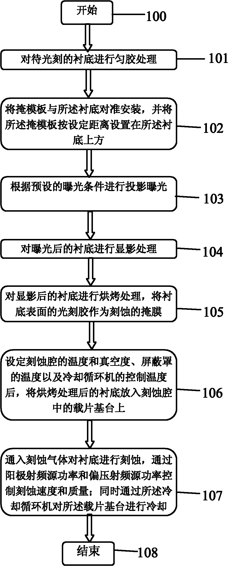
[0028] exist figure 1The flow chart of the first preferred embodiment of the method for producing a patterned sapphire substrate of the present invention shown; The substrate is subjected to glue leveling treatment; then to the next step 102, the mask plate is aligned with the substrate and installed, and the mask plate is placed on the substrate at a set distance; then to the next step 103, according to Perform projection exposure under preset exposure conditions; then go to the next step 104 to develop the exposed substrate; then go to the next step 105 to bake the developed substrate to remove ...


PUM


Abstract

The invention relates to a method for manufacturing a graphical sapphire substrate. The method comprises the following steps of: performing spin-coating treatment on a substrate to be photoetched; aligning and installing a mask plate and the substrate and installing the mask plate above the substrate according to set distance; performing projection exposure according to preset exposure conditions; performing developing treatment on the exposed substrate; performing roasting treatment on the developed substrate, and taking photoresist on the surface of the substrate as an etching mask; after setting the temperature and the vacuum degree of an etching cavity, the temperature of a shield cover and the control temperature of a cooling circulation mechanism, placing the roasted substrate on a slide glass base station in the etching cavity; introducing an etching gas for etching the substrate; controlling etching speed and quality by anode radio frequency source power and bias radio frequency source power; and simultaneously, cooling the slide glass base station by using the cooling circulation mechanism. By the method, the graphical substrate production efficiency is high and the luminous efficiency of a chip produced by using the substrate is high and stable.

Description

technical field [0001] The invention relates to the field of manufacturing sapphire substrates, in particular to a method for manufacturing patterned sapphire substrates. Background technique [0002] In order to improve the luminous intensity of LED lighting, it is necessary to improve the photoelectric conversion efficiency of LED. The photoelectric conversion efficiency of LED includes two parts: internal quantum efficiency and external quantum efficiency. Efficiency; external quantum efficiency refers to the total efficiency after the photons generated in the LED junction area are extracted from the LED. Most of the sapphire substrates currently used for GaN growth are C-Plane sapphire substrates. This is mainly because the process of growing sapphire crystals along the C-axis is mature, the cost is relatively low, and the physical and chemical properties are stable. The technology for epitaxy on the C-plane is mature. Stablize. However, the GaN film grown on the C-pla...

Claims


Application Information

Patent Timeline
Patent Type & Authority Applications(China)
IPC IPC(8): H01L33/00G03F7/20G03F7/40
Inventor 谢雪峰李明远郭爱华
Owner 长治虹源科技晶体有限公司
Why Eureka
Try Eureka