Low-loss medium loaded surface plasmon excimer optical waveguide

A surface plasmon, dielectric loading type technology, applied in the field of optical waveguide, can solve the problems of unfavorable waveguide and device integration, increased transmission loss, long transmission distance, etc., and achieves the effect of size reduction, transmission loss reduction, and low transmission loss.

Inactive Publication Date: 2011-08-31
BEIHANG UNIV
View PDF2 Cites 17 Cited by
  • Summary
  • Abstract
  • Description
  • Claims
  • Application Information

AI Technical Summary

Problems solved by technology

Such waveguides enable low-loss optical signal transmission but tend to be relatively large in size
Usually, in order to ensure single-mode conditions and maintain a long transmission distance, the length and width of the polymer cross-section are often around 600 nanometers, and the corresponding mode field size has reached the order of ne

Method used


Image

  • Low-loss medium loaded surface plasmon excimer optical waveguide
  • Low-loss medium loaded surface plasmon excimer optical waveguide
  • Low-loss medium loaded surface plasmon excimer optical waveguide

Examples


example 1

[0036] Example 1: Optical waveguide structure with large difference in refractive index of materials in high and low refractive index medium regions

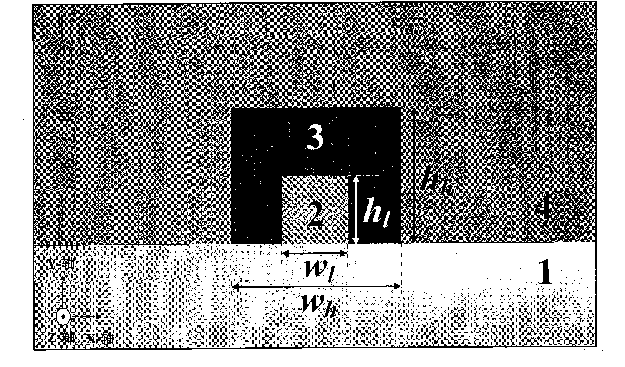
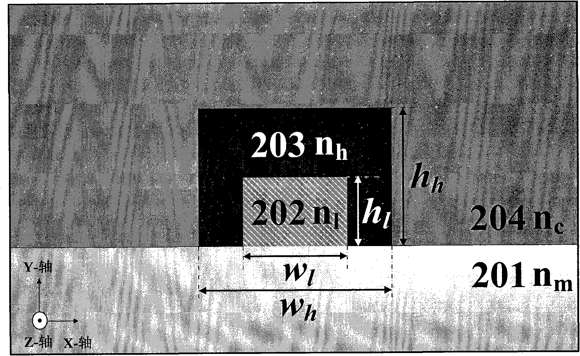
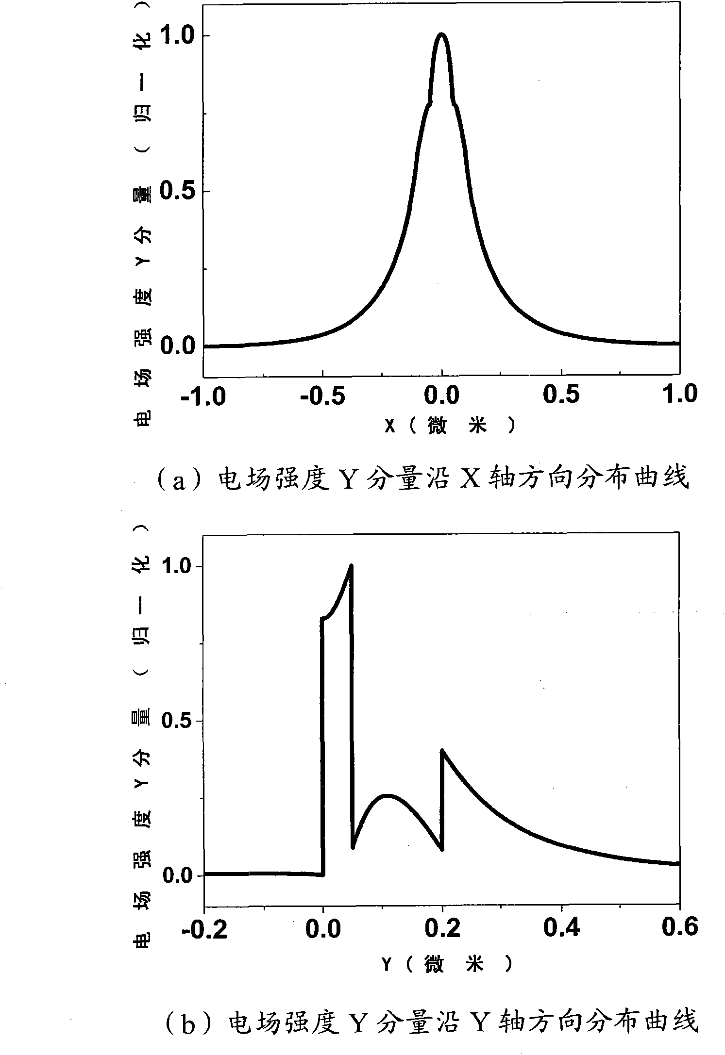
[0037] figure 2 It is the structural diagram of the dielectric-loaded surface plasmon optical waveguide described in Example 1. 201 is the metal base layer, n m Its refractive index; 202 is the low refractive index medium area, n 1 is its refractive index, W l its width, h l Its height; 203 is the high emissivity medium area, n h is its refractive index, W h its width, h h Its height; 204 is cladding, n c for its refractive index.

[0038] In this example, the wavelength of the transmitted optical signal is selected as 1.55 μm, the material of 201 is silver, and the refractive index at the wavelength of 1.55 μm is 0.1453+i*11.3587; the material of 202 is set as air, and its refractive index is 1 ; The material of 203 is silicon, whose refractive index is 3.5; the material of 204 is silicon dioxide, whose refractive ind...

example 2

[0045] Example 2: Optical waveguide structure with small difference in refractive index of materials in high and low refractive index medium regions

[0046] The structural diagram of the dielectric-loaded surface plasmon optical waveguide described in Example 2 is shown in figure 2 . 201 is the metal base layer, n m Its refractive index; 202 is the low refractive index medium area, n 1 is its refractive index, W l its width, h l Its height; 203 is the high emissivity medium area, n h is its refractive index, W h its width, h h Its height; 204 is cladding, n c for its refractive index.

[0047] In this example, the wavelength of the transmitted optical signal is selected as 1.55 μm, the material of 201 is silver, and the refractive index at the wavelength of 1.55 μm is 0.1453+i*11.3587; the material of 202 is silicon nitride, and its refractive index 2; the material of 203 is silicon, whose refractive index is 3.5; the material of 204 is silicon dioxide, whose refrac...


PUM

PropertyMeasurementUnit
Widthaaaaaaaaaa

Abstract

The invention discloses a medium loaded surface plasmon excimer optical waveguide with low transmission loss and stronger light-field limiting ability. In the invention, the cross section of the waveguide structure comprises a metal basal layer (1), a high refractive index medium region (3) located on the metal basal layer, a low refractive index medium region (2) surrounded by the high refractive index medium region and the metal basal layer and a cladding (4), wherein the light-field distribution range of the waveguide structure can be obviously reduced by the high refractive index medium region on the metal basal layer so that the two-dimensional sub-wavelength constraint to a transmission light field is realized; and in the meantime, as the existence of the low refractive index medium region, the lower transmission loss of the waveguide can be maintained. By means of the optical waveguide structure, the contradiction of the light-field limiting ability and the transmission lost of a conventional medium loaded surface plasmon excimer optical waveguide is overcome and an ultrahigh integration level optical waveguide chip is possible to realize.

Description

technical field [0001] The invention relates to the technical field of optical waveguides, in particular to a low-loss dielectric-loaded surface plasmon optical waveguide. Background technique [0002] A surface plasmon is a pattern of electromagnetic waves caused by the interaction of light and free electrons on the surface of a metal. This mode exists near the metal-dielectric interface, and its field strength reaches its maximum at the interface, and decays exponentially on both sides of the interface along the direction perpendicular to the interface. Surface plasmons have strong field confinement properties, which can confine the field energy to a region whose spatial size is much smaller than its free-space transmission wavelength, and its properties can change with the change of the metal surface structure. In the surface plasmon optical waveguide structure composed of appropriate metal and dielectric, the transverse optical field distribution can be limited to a ran...

Claims


Application Information

Patent Timeline
IPC IPC(8): G02B6/10
Inventor 郑铮卞宇生刘娅朱劲松
Owner BEIHANG UNIV
Why Eureka
Try Eureka