

TFT-LCD (thin film transistor liquid crystal display) pixel electrode layer structure, preparation method and mask plate thereof
A pixel electrode layer and pixel electrode technology, applied in the direction of circuits, electrical components, electrical solid devices, etc., can solve the problems of lower product yield, abnormal display, and lower panel display quality, so as to avoid twill mura and reduce Effect of difference in developer concentration
- Summary
- Abstract
- Description
- Claims
- Application Information
AI Technical Summary
Problems solved by technology
Method used
Image

Examples
Embodiment 1
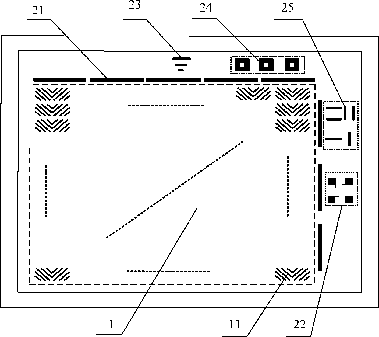
[0038] Since in the development process of preparing the pixel electrode layer, in the non-display area, the area of the peripheral area pattern is small. Therefore, taking the positive photoresist as an example, the photoresist area that needs to be reserved in the non-display area is also small. Most photoresist reacts with the developer and consumes more developer. In the display area, the remaining photoresist area is larger and consumes less developer. Therefore, the periphery of the panel (non-display area) and the panel The concentration of the developer in the center (display area) is different, which leads to uneven distribution of the developer concentration on the entire panel. The developer concentration at the periphery of the panel is much smaller than the developer concentration in the center of the panel, which causes the developer in the center of the panel to flow toward the panel. Peripheral diffusion causes the DI CD to be affected by the developer concentr...
Embodiment 2
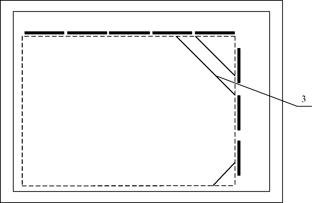
[0045] On the basis of embodiment 1, further, such as image 3 As shown, the peripheral filling graphics 4 and the graphics included in the peripheral area graphics are not connected to each other and independent of each other. In order to avoid interference between the surrounding filling pattern and the graphics contained in the surrounding area pattern, affecting the function of the surrounding area pattern, making the surrounding filling pattern and the peripheral driving circuit part, the pattern for process detection, the pattern for mask alignment, etc. mutually different The connection makes the original surrounding area graphics and the surrounding filling graphics independent of each other.
[0046] Furthermore, after the mask provided in this embodiment is used for exposure, the proportion of the photoresist remaining in the display area and the non-display area is difficult to guarantee to be completely consistent, so the pattern 4 and the pixel electrode are filled in...
Embodiment 3
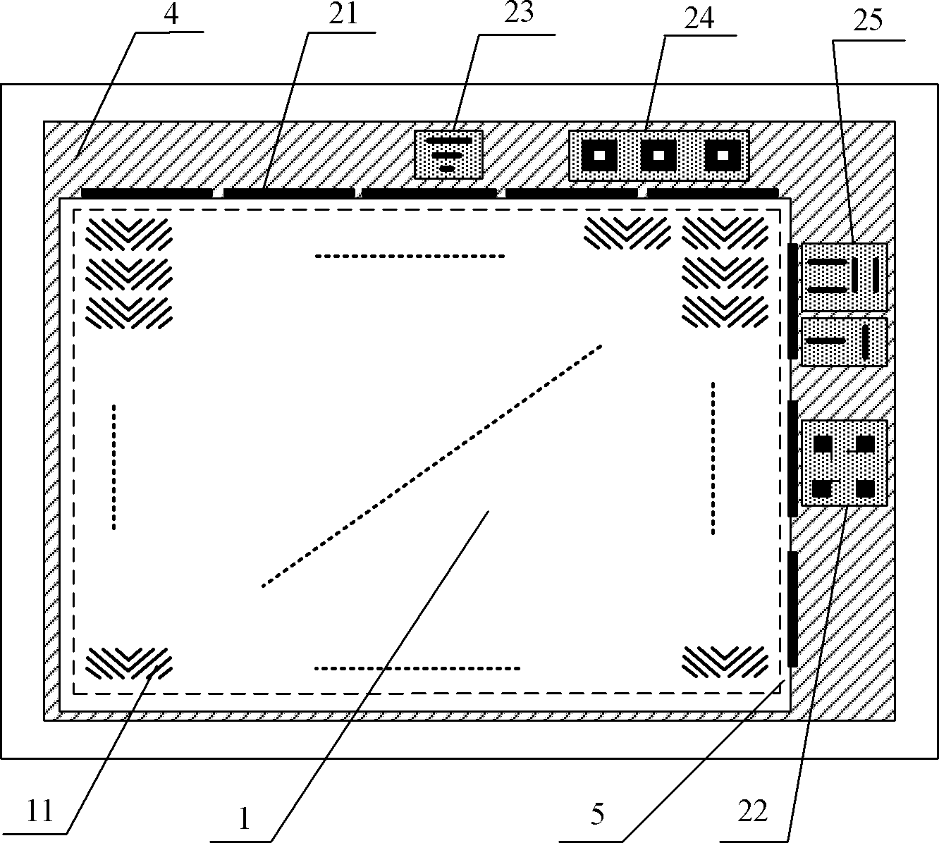
[0049] Increase the area of the pattern to be retained in the peripheral area, that is, set the pattern of the peripheral filling pattern, so that the area of the photoresist to be retained is more appropriate, so that the developer concentration in the peripheral area during the development process is the same as the developer concentration in the display area. Since the area of the peripheral area graphics is small, the effect of the difference of the graphics is also small. Therefore, on the basis of the above embodiment, further, the peripheral filling pattern can be set to be the same as the pattern texture of the pixel electrode pattern. In this way, to the greatest extent, the developer concentration in the peripheral area during the development process is the same as the developer concentration in the display area.
[0050] Since the developer concentration in the peripheral area during the development process cannot be completely consistent with the developer concen...
PUM
 Abstract
Description
Claims
Application Information